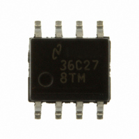
DS36C278TM/NOPB National Semiconductor, DS36C278TM/NOPB Datasheet - Page 4

DS36C278TM/NOPB
Manufacturer Part Number
DS36C278TM/NOPB
Description
IC TRANSCEIVER EIA LP 8-SOIC
Manufacturer
National Semiconductor
Type
Transceiverr
Datasheet
1.DS36C278TMNOPB.pdf
(10 pages)
Specifications of DS36C278TM/NOPB
Number Of Drivers/receivers
1/1
Protocol
RS485
Voltage - Supply
4.75 V ~ 5.25 V
Mounting Type
Surface Mount
Package / Case
8-SOIC (3.9mm Width)
Number Of Receivers
1
Number Of Transmitters
1
Number Of Transceivers
1
Data Transmission Topology
Multipoint
Receiver Signal Type
Differential
Transmitter Signal Type
Differential
Single Supply Voltage (typ)
5V
Single Supply Voltage (min)
4.75V
Single Supply Voltage (max)
5.25V
Dual Supply Voltage (typ)
Not RequiredV
Dual Supply Voltage (min)
Not RequiredV
Dual Supply Voltage (max)
Not RequiredV
Supply Current
0.5mA
Power Supply Requirement
Single
Operating Temp Range
-40C to 85C
Operating Temperature Classification
Industrial
Mounting
Surface Mount
Pin Count
8
Package Type
SOIC N
Lead Free Status / RoHS Status
Lead free / RoHS Compliant
Other names
*DS36C278TM
*DS36C278TM/NOPB
DS36C278TM
*DS36C278TM/NOPB
DS36C278TM
Available stocks
Company
Part Number
Manufacturer
Quantity
Price
Company:
Part Number:
DS36C278TM/NOPB
Manufacturer:
NS
Quantity:
1 524
www.national.com
Switching Characteristics
Note 2: “Absolute Maximum Ratings” are those values beyond which the safety of the device cannot be guaranteed. They are not meant to imply that the devices
should be operated at these limits. The table of “Electrical Characteristics” specifies conditions of device operation.
Note 3: Current into device pins is defined as positive. Current out of device pins is defined as negative. All voltages are referenced to ground except V
V
Note 4: All typicals are given for: V
Note 5: Delta |V
Note 6: Threshold parameter limits specified as an algebraic value rather than by magnitude.
Note 7: Hysteresis defined as V
Note 8: I
Note 9: C
Note 10: For complete details of test, see RS-485.
Parameter Measurement Information
Vtest = −7V to +12V
OD2
.
IN
L
includes the receiver input current and driver TRI-STATE leakage current.
includes probe and jig capacitance.
FIGURE 1. Driver V
OD2
FIGURE 3. Driver V
| and Delta |V
FIGURE 2. Driver V
FIGURE 4. Driver I
HST
OC
CC
| are changes in magnitude of V
= V
= +5.0V, T
TH
OD2
OH
− V
TL
and V
OSD
and V
OD3
.
A
01204002
= + 25˚C.
(Notes 4, 9) (Continued)
OL
OC
01204004
01204018
01204003
OD2
and V
OC
4
, respectively, that occur when input changes state.
FIGURE 6. Driver Differential Propagation Delays and
FIGURE 5. Driver Differential Propagation Delay Test
Differential Rise and Fall Times
Circuit
01204006
01204005
OD1
and


