MC1488DR2G ON Semiconductor, MC1488DR2G Datasheet - Page 3
MC1488DR2G
Manufacturer Part Number
MC1488DR2G
Description
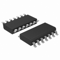
IC LINE DRIVER QUAD MONO 14-SOIC
Manufacturer
ON Semiconductor
Type
Line Driver, Transmitterr
Datasheet
1.MC1488PG.pdf
(11 pages)
Specifications of MC1488DR2G
Number Of Drivers/receivers
4/0
Protocol
RS232
Voltage - Supply
15V
Mounting Type
Surface Mount
Package / Case
14-SOIC (3.9mm Width), 14-SOL
Maximum Operating Temperature
+ 75 C
Mounting Style
SMD/SMT
Interface
EIA-232-D
Minimum Operating Temperature
0 C
Number Of Lines (input / Output)
/ /
Supply Current
34 mA
Lead Free Status / RoHS Status
Lead free / RoHS Compliant
Other names
MC1488DR2GOS
MC1488DR2GOS
MC1488DR2GOSTR
MC1488DR2GOS
MC1488DR2GOSTR
Available stocks
Company
Part Number
Manufacturer
Quantity
Price
Company:

Part Number:
MC1488DR2G
Manufacturer:
ON
Quantity:
13 533
Part Number:
MC1488DR2G
Manufacturer:
ON/安森美
Quantity:
20 000


Stresses exceeding Maximum Ratings may damage the device. Maximum Ratings are stress ratings only. Functional operation above the
Recommended Operating Conditions is not implied. Extended exposure to stresses above the Recommended Operating Conditions may affect
device reliability.
MAXIMUM RATINGS
ELECTRICAL CHARACTERISTICS
SWITCHING CHARACTERISTICS
1. Maximum Package Power Dissipation may be exceeded if all outputs are shorted simultaneously.
Power Supply Voltage
Input Voltage Range
Output Signal Voltage
Power Derating (Package Limitation, SO−14 and Plastic Dual−In−Line Package)
Operating Ambient Temperature Range
Storage Temperature Range
Input Current − Low Logic State (V
Input Current − High Logic State (V
Output Voltage − High Logic State
Output Voltage − Low Logic State
Positive Output Short−Circuit Current, Note 1
Negative Output Short−Circuit Current, Note 1
Output Resistance (V
Positive Supply Current (R
Negative Supply Current (R
Power Consumption
Propagation Delay Time (z
Fall Time
Propagation Delay Time (z
Rise Time
Derate above T
(V
(V
(V
(V
(V
(V
(V
(V
(V
(V
(V
(V
(V
(V
(V
(V
(V
(V
IL
IL
IH
IH
IH
IL
IH
IL
IH
IL
IH
IL
IH
IL
IH
IL
CC
CC
= 0.8 Vdc, R
= 0.8 Vdc, R
= 0.8 Vdc, V
= 0.8 Vdc, V
= 0.8 Vdc, V
= 0.8 Vdc, V
= 0.8 Vdc, V
= 0.8 Vdc, V
= 1.9 Vdc, R
= 1.9 Vdc, R
= 1.9 Vdc, V
= 1.9 Vdc, V
= 1.9 Vdc, V
= 1.9 Vdc, V
= 1.9 Vdc, V
= 1.9 Vdc, V
= 9.0 Vdc, V
= 12 Vdc, V
A
CC
CC
CC
EE
EE
EE
L
L
L
L
CC
CC
CC
EE
EE
EE
= + 25°C
EE
EE
= 3.0 kW , V
= 3.0 kW , V
= 3.0 kW , V
= 3.0 kW , V
CC
= − 9.0 Vdc)
= − 12 Vdc)
= − 15 Vdc)
= + 9.0 Vdc)
= + 12 Vdc)
= + 15 Vdc)
= − 9.0 Vdc)
= − 12 Vdc)
= − 15 Vdc)
= + 9.0 Vdc)
= + 12 Vdc)
= + 15 Vdc)
= − 12 Vdc)
= − 9.0 Vdc)
(T
= V
A
(z
(z
I
L
= ∞)
= + 25°C, unless otherwise noted.)
Characteristic
I
I
I
I
EE
= ∞)
= 3.0 k and 15 pF)
= 3.0 k and 15 pF)
= 3.0 k and 15 pF)
= 3.0 k and 15 pF)
= 0, ⎥ V
CC
CC
CC
CC
IL
IH
= + 9.0 Vdc, V
= + 13.2 Vdc, V
= + 9.0 Vdc, V
= + 13.2 Vdc, V
= 0)
= 5.0 V)
O
(V
⎜ = ± 2.0 V)
(V
CC
CC
Rating
= + 9.0 ± 1% Vdc, V
= + 9.0 ± 1% Vdc, V
EE
EE
EE
EE
= − 9.0 Vdc)
= − 9.0 Vdc)
= − 13.2 Vdc)
= − 13.2 Vdc)
http://onsemi.com
EE
EE
3
= − 9.0 ± 1% Vdc, T
= − 9.0 ± 1% Vdc, T
Symbol
I
I
V
t
t
t
t
V
OS +
OS −
I
I
P
PLH
THL
PHL
TLH
I
I
CC
r
EE
IH
OH
IL
OL
o
C
A
A
= + 25°C.)
+ 6.0
+ 9.0
− 6.0
− 9.0
+ 6.0
− 6.0
Min
300
= 0 to 75°C, unless otherwise noted.)
−
−
−
−
−
−
−
−
−
−
−
−
−
−
−
−
−
−
−
−
Symbol
1/R
+ 10.5
− 10.5
− 7.0
+ 4.5
+ 5.5
+ 7.0
+ 10
− 10
+ 15
+ 19
− 13
− 18
V
V
T
Typ
275
110
V
V
1.0
P
T
45
55
stg
−
−
−
−
−
−
−
−
−
−
CC
EE
IR
O
A
D
qJA
− 15 p V
− 65 to + 175
0 to + 75
− 500
− 500
+ 6.0
+ 7.0
Value
− 2.5
Max
+ 12
− 12
+ 20
+ 25
+ 34
+ 12
− 17
− 23
− 34
1000
333
576
350
175
100
+ 15
− 15
± 15
1.6
10
75
7.0
6.7
−
−
−
−
−
IR
p
Ohms
mW/°C
Unit
Vdc
Vdc
mW
mA
mA
mA
mA
mA
mA
mA
mA
Unit
mW
mA
mA
mA
Vdc
Vdc
Vdc
ns
ns
ns
ns
°C
°C
Related parts for MC1488DR2G
Image
Part Number
Description
Manufacturer
Datasheet
Request
R

Part Number:
Description:
CONTACTOR, 1NO, 110VAC, 14A, DIN RAIL
Manufacturer:
IMO PRECISION CONTROLS
Datasheet:
Part Number:
Description:
CONTACTOR, 1NO, 230VAC, 14A, DIN RAIL
Manufacturer:
IMO PRECISION CONTROLS
Datasheet:
Part Number:
Description:
CONTACTOR, 1NO, 24VAC, 14A, DIN RAIL
Manufacturer:
IMO PRECISION CONTROLS
Datasheet:

Part Number:
Description:
ON Semiconductor [VOLTAGE REGULATOR]
Manufacturer:
ON Semiconductor
Datasheet:
Part Number:
Description:
357-036-542-201 CARDEDGE 36POS DL .156 BLK LOPRO
Manufacturer:
ON Semiconductor
Datasheet:
Part Number:
Description:
357-036-542-201 CARDEDGE 36POS DL .156 BLK LOPRO
Manufacturer:
ON Semiconductor
Datasheet:
Part Number:
Description:
357-036-542-201 CARDEDGE 36POS DL .156 BLK LOPRO
Manufacturer:
ON Semiconductor
Datasheet:
Part Number:
Description:
357-036-542-201 CARDEDGE 36POS DL .156 BLK LOPRO
Manufacturer:
ON Semiconductor
Datasheet:
Part Number:
Description:
357-036-542-201 CARDEDGE 36POS DL .156 BLK LOPRO
Manufacturer:
ON Semiconductor
Datasheet:
Part Number:
Description:
357-036-542-201 CARDEDGE 36POS DL .156 BLK LOPRO
Manufacturer:
ON Semiconductor
Datasheet:
Part Number:
Description:
357-036-542-201 CARDEDGE 36POS DL .156 BLK LOPRO
Manufacturer:
ON Semiconductor
Datasheet:
Part Number:
Description:
357-036-542-201 CARDEDGE 36POS DL .156 BLK LOPRO
Manufacturer:
ON Semiconductor
Datasheet:
Part Number:
Description:
357-036-542-201 CARDEDGE 36POS DL .156 BLK LOPRO
Manufacturer:
ON Semiconductor
Datasheet: