MAX4950ACTX+ Maxim Integrated Products, MAX4950ACTX+ Datasheet - Page 4
MAX4950ACTX+
Manufacturer Part Number
MAX4950ACTX+
Description
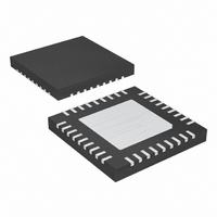
IC PCIE REDRIVER DUAL 36-TQFN
Manufacturer
Maxim Integrated Products
Type
Equalizerr
Specifications of MAX4950ACTX+
Voltage - Supply
3.3V
Mounting Type
Surface Mount
Package / Case
36-TQFN Exposed Pad
Supply Voltage (max)
3.6 V
Supply Voltage (min)
3 V
Maximum Operating Temperature
+ 70 C
Mounting Style
SMD/SMT
Minimum Operating Temperature
0 C
Propagation Delay Time
280 ps
Supply Voltage Range
3V To 3.6V
Operating Temperature Range
0°C To +70°C
Digital Ic Case Style
TQFN
No. Of Pins
36
Peak Reflow Compatible (260 C)
Yes
Termination Type
SMD
Rohs Compliant
Yes
Filter Terminals
SMD
Leaded Process Compatible
Yes
No. Of Channels
2
Lead Free Status / RoHS Status
Lead free / RoHS Compliant
Number Of Drivers/receivers
-
Protocol
-
Lead Free Status / Rohs Status
Lead free / RoHS Compliant


Dual PCI Express Equalizer/Redriver
ELECTRICAL CHARACTERISTICS (continued)
(V
otherwise noted. Typical values are at V
Note 3: All devices are 100% production tested at T
Note 4: Currents are applicable for both PCIe Generation I and Generation II speeds. Table 5 summarizes the predicted power
Note 5: Guaranteed by design, unless otherwise noted.
Note 6: Equivalent to the same amount of deemphasis driving the output.
Note 7: Rise and fall times are measured using 20% and 80% levels.
Figure 1. Illustration of Output Deemphasis
4
Electrical Idle Detect Threshold
Output Voltage During Electrical
Idle (AC)
Receiver Detect Pulse
Amplitude (Note 5)
Receiver Detect Pulse Width
Receiver Detect Retry Period
CONTROL LOGIC (INEQ_1, INEQ_0, ODE_1, ODE_0, EN, RX_DET, O_AMP_)
Input Logic-Level Low
Input Logic-Level High
Input Logic Hysteresis
Input Leakage Current
CC
_______________________________________________________________________________________
= +3.0V to +3.6V, C
consumption.
PARAMETER
CL
= 75nF coupling capacitor on each output, R
SYMBOL
V
V
DIFF-AC-P
V
THRESH
DETECT
TX-IDLE-
TX-IDLE-
TX-RCV-
V
CC
HYST
V
V
I
IN
IH
IL
= +3.3V and T
ABS|V
Voltage change in positive direction
V
CONTROL_LOGIC
A
= +70°C. Specifications for all temperature limits are guaranteed by design.
PE(dB) = 20
OUT_P
A
= +25°C.) (Note 3)
- V
V
LOW_P-P
[
CONDITIONS
log
OUT_M
(
= +0.5V or +1.5V
V
V
HIGH_P-P
LOW_P-P
V
|, f = 500MHz
HIGH_P-P
L
)]
= 50Ω resistor on each output, T
MIN
1.4
-50
65
Timing Diagram
TYP
100
130
200
95
A
= 0°C to +70°C, unless
MAX
+50
120
600
0.6
25
UNITS
mV
mV
mV
mV
μA
ns
ns
V
V
P-P
P-P
Related parts for MAX4950ACTX+
Image
Part Number
Description
Manufacturer
Datasheet
Request
R

Part Number:
Description:
MAX7528KCWPMaxim Integrated Products [CMOS Dual 8-Bit Buffered Multiplying DACs]
Manufacturer:
Maxim Integrated Products
Datasheet:
Part Number:
Description:
Single +5V, fully integrated, 1.25Gbps laser diode driver.
Manufacturer:
Maxim Integrated Products
Datasheet:
Part Number:
Description:
Single +5V, fully integrated, 155Mbps laser diode driver.
Manufacturer:
Maxim Integrated Products
Datasheet:
Part Number:
Description:
VRD11/VRD10, K8 Rev F 2/3/4-Phase PWM Controllers with Integrated Dual MOSFET Drivers
Manufacturer:
Maxim Integrated Products
Datasheet:
Part Number:
Description:
Highly Integrated Level 2 SMBus Battery Chargers
Manufacturer:
Maxim Integrated Products
Datasheet:
Part Number:
Description:
Current Monitor and Accumulator with Integrated Sense Resistor; ; Temperature Range: -40°C to +85°C
Manufacturer:
Maxim Integrated Products
Part Number:
Description:
TSSOP 14/A�/RS-485 Transceivers with Integrated 100O/120O Termination Resis
Manufacturer:
Maxim Integrated Products
Part Number:
Description:
TSSOP 14/A�/RS-485 Transceivers with Integrated 100O/120O Termination Resis
Manufacturer:
Maxim Integrated Products
Part Number:
Description:
QFN 16/A�/AC-DC and DC-DC Peak-Current-Mode Converters with Integrated Step
Manufacturer:
Maxim Integrated Products
Part Number:
Description:
TDFN/A/65V, 1A, 600KHZ, SYNCHRONOUS STEP-DOWN REGULATOR WITH INTEGRATED SWI
Manufacturer:
Maxim Integrated Products
Part Number:
Description:
Integrated Temperature Controller f
Manufacturer:
Maxim Integrated Products
Part Number:
Description:
SOT23-6/I�/45MHz to 650MHz, Integrated IF VCOs with Differential Output
Manufacturer:
Maxim Integrated Products
Part Number:
Description:
SOT23-6/I�/45MHz to 650MHz, Integrated IF VCOs with Differential Output
Manufacturer:
Maxim Integrated Products
Part Number:
Description:
EVALUATION KIT/2.4GHZ TO 2.5GHZ 802.11G/B RF TRANSCEIVER WITH INTEGRATED PA
Manufacturer:
Maxim Integrated Products
Part Number:
Description:
QFN/E/DUAL PCIE/SATA HIGH SPEED SWITCH WITH INTEGRATED BIAS RESISTOR
Manufacturer:
Maxim Integrated Products
Datasheet: