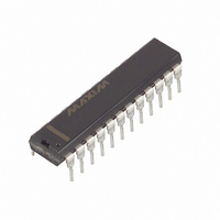
MAX1490EBCPG+ Maxim Integrated Products, MAX1490EBCPG+ Datasheet - Page 4

MAX1490EBCPG+
Manufacturer Part Number
MAX1490EBCPG+
Description
IC RS485/RS422 DATA INTRFC 24DIP
Manufacturer
Maxim Integrated Products
Type
Transceiverr
Datasheet
1.MAX1480ECEPI.pdf
(19 pages)
Specifications of MAX1490EBCPG+
Number Of Drivers/receivers
1/1
Protocol
RS422, RS485
Voltage - Supply
4.5 V ~ 5.5 V
Mounting Type
Through Hole
Package / Case
24-DIP (0.600", 15.24mm)
Data Rate
250 Kbps
Operating Supply Voltage
5 V
Supply Current
130 mA
Operating Temperature Range
0 C to + 70 C
Maximum Power Dissipation
696 mW
Mounting Style
Through Hole
Lead Free Status / RoHS Status
Lead free / RoHS Compliant
SWITCHING CHARACTERISTICS—MAX1480EA/MAX1490EA (continued)
(V
SWITCHING CHARACTERISTICS—MAX1480EC/MAX1490EB
(V
±15kV ESD-Protected, Isolated RS-485/RS-422
Data Interfaces
4
Note 1: All currents into device pins are positive; all currents out of device pins are negative. All voltages are referenced to logic-
Note 2: For DE
Note 3: Shutdown supply current is the current at V
Note 4: Limit guaranteed by applying 1520V
Note 5: Applies to peak current (see Typical Operating Characteristics). Although the MAX1480EA/MAX1480EC and
|t
Receiver Skew
Maximum Data Rate
Time to Shutdown
Shutdown to Driver Output High
Shutdown to Driver Output Low
Driver Input to Output
Propagation Delay
Driver Output Skew
Driver Rise or Fall Time
Driver Enable to Output High
(MAX1480EC Only)
Driver Enable to Output Low
(MAX1480EC Only)
Driver Disable Time from Low
(MAX1480EC Only)
Driver Disable Time from High
(MAX1480EC Only)
Receiver Input to Output
Propagation Delay
|t
Receiver Skew
Maximum Data Rate
Time to Shutdown
Shutdown to Driver Output High
Shutdown to Driver Output Low
CC_
CC_
PLH
PLH
_______________________________________________________________________________________
= +5V ±10%, V
= +5V ±10%, V
- t
- t
PHL
PHL
side ground (GND_), unless otherwise specified.
MAX1480EC, Figure 2 for MAX1490EA/MAX1490EB).
pins on the other side of the package, e.g., between pins 1–14 and pins 15–28 on the 28-pin package.
MAX1490EA/MAX1490EB provide electrical isolation between logic ground and signal paths, they do not provide isolation
between external shields and the signal paths (see Isolated Common Connection section).
PARAMETER
PARAMETER
| Differential
| Differential
´
and DI
FS
FS
´
= V
= V
pin descriptions, see Detailed Block Diagram and Typical Application Circuit (Figure 1 for MAX1480EA/
CC_
CC_
, T
, T
A
A
t
t
t
SYMBOL
SYMBOL
t
ZH(SHDN)
ZH(SHDN)
ZH(SHDN)
= T
= T
ZL(SHDN)
t
t
t
f
SHDN
SKEW
t
f
SHDN
t
t
t
t
t
t
SKD
MAX
R,
SKD
MAX
PLH
PHL
t
t
t
t
PLH
PHL
ZH
HZ
ZL
LZ
MIN
MIN
t
F
to T
to T
RMS
MAX
MAX
Figures 5 and 10, R
t
Figures 6 and 9, C
Figures 6 and 9, C
Figures 5 and 7, R
Figures 5 and 7, R
Figures 5 and 7, R
Figures 5 and 7, R
Figures 6 and 8, C
Figures 6 and 8, C
Figures 6 and 8, C
Figures 6 and 8, C
Figures 5 and 10, R
Figures 5 and 10, R
t
Figures 6 and 9, C
Figures 6 and 9, C
SKEW
SKEW
for 1s. Test voltage is applied between all pins on one side of the package to all
, unless otherwise noted. Typical values are at V
, unless otherwise noted. Typical values are at V
CC1
, t
, t
SKD
SKD
and V
, t
≤ 25% of data period
PHL
CC2
CONDITIONS
CONDITIONS
≤ 25% of data period
DIFF
DIFF
DIFF
DIFF
L
L
L
L
L
L
L
L
when shutdown is enabled.
DIFF
DIFF
DIFF
= 100pF, S2 closed
= 100pF, S1 closed
= 100pF, S2 closed
= 100pF, S1 closed
= 15pF, S1 closed
= 15pF, S2 closed
= 100pF, S2 closed
= 100pF, S1 closed
= 54Ω, C
= 54Ω, C
= 54Ω, C
= 54Ω, C
= 54Ω, C
= 54Ω, C
= 54Ω, C
L1
L1
L1
L1
L1
L1
L1
= C
= C
= C
= C
= C
= C
= C
L2
L2
L2
L2
L2
L2
L2
= 100pF
= 100pF
= 100pF
= 100pF
= 100pF
= 100pF
= 100pF
CC_
CC_
MIN
MIN
160
2.5
= +5V and T
= +5V and T
TYP
TYP
100
300
200
100
1.4
1.1
1.0
1.4
1.4
2.0
1.7
0.9
1.1
30
3
3
3
3
A
A
MAX
MAX
1200
150
= +25°C.)
= +25°C.)
3.0
3.0
2.0
4.5
4.5
4.5
4.5
3.0
3.0
15
15
15
15
UNITS
UNITS
Mbps
kbps
ns
µs
µs
µs
µs
ns
µs
µs
µs
µs
µs
µs
ns
µs
µs
µs


