FIN1048MTCX Fairchild Semiconductor, FIN1048MTCX Datasheet
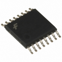
IC RCVR QUAD3.3V LVDS HS 16TSSOP

FIN1048MTCX

Manufacturer Part Number
FIN1048MTCX
Description
IC RCVR QUAD3.3V LVDS HS 16TSSOP
Manufacturer
Fairchild Semiconductor
Type
Receiverr
Datasheet

Specifications of FIN1048MTCX

Number Of Drivers/receivers
0/4
Protocol
LVDS
Voltage - Supply
3 V ~ 3.6 V
Mounting Type
Surface Mount
Package / Case
16-TSSOP
Number Of Elements
4
Number Of Receivers
4
Number Of Drivers
4
Operating Supply Voltage (typ)
3.3V
Differential Input High Threshold Voltage
100mV
Diff. Input Low Threshold Volt
-100mV
Transmission Data Rate
400Mbps
Propagation Delay Time
2.5ns
Operating Temp Range
-40C to 85C
Operating Temperature Classification
Industrial
Mounting
Surface Mount
Pin Count
16
Package Type
TSSOP
Logic Family
FIN10
Logic Type
High Speed Differential Receiver
Supply Voltage (max)
3.6 V
Supply Voltage (min)
3 V
Maximum Operating Temperature
+ 85 C
Mounting Style
SMD/SMT
Data Rate
400 Mbps
Interface
EIA/TIA-644. RS-422
Minimum Operating Temperature
- 40 C
Number Of Lines (input / Output)
/ /
Supply Current
15 mA
Lead Free Status / RoHS Status
Lead free / RoHS Compliant

Available stocks

Company
Part Number
Manufacturer
Quantity
Price
Part Number:
FIN1048MTCX
Manufacturer:
FSC
Quantity:
5 000
Part Number:
FIN1048MTCX
Manufacturer:
FAIRCHILD/仙童
Quantity:
20 000
© 2003 Fairchild Semiconductor Corporation
FIN1048M
FIN1048MTC
FIN1048
3.3V LVDS 4-Bit Flow-Through
High Speed Differential Receiver
General Description
This quad receiver is designed for high speed interconnect
utilizing Low Voltage Differential Signaling (LVDS) technol-
ogy. The receiver translates LVDS levels, with a typical dif-
ferential input threshold of 100mV, to LVTTL signal levels.
LVDS provides low EMI at ultra low power dissipation even
at high frequencies. This device is ideal for high speed
transfer of clock and data.
The FIN1048 can be paired with its companion driver, the
FIN1047, or any other LVDS driver.
Ordering Code:
Devices also available in Tape and Reel. Specify by appending the suffix letter “X” to the ordering code.
Connection Diagram
Order Number
Package Number
MTC16
M16A
16-Lead Small Outline Integrated Circuit (SOIC), JEDEC MS-012, 0.150" Narrow
16-Lead Thin Shrink Small Outline Package (TSSOP), JEDEC MO-153, 4.4mm Wide
DS500588
Features
Pin Descriptions
Function Table
H
Z
R
Greater than 400Mbs data rate
Flow-through pinout simplifies PCB layout
3.3V power supply operation
0.4ns maximum differential pulse skew
2.5ns maximum propagation delay
Low power dissipation
Power-Off protection
Fail safe protection for open-circuit, shorted and termi-
nated conditions
Meets or exceeds the TIA/EIA-644 LVDS standard
Pin compatible with equivalent RS-422 and LVPECL
devices
16-Lead SOIC and TSSOP packages save space
OUT1
High Impedance
HIGH Logic Level
R
R
L or Open
IN1
IN1
Package Description
EN
, R
H
H
H
X
, R
, R
OUT2
Pin Name
IN2
IN2
GND
V
EN
EN
, R
, R
, R
CC
L or Open
L or Open
L or Open Fail Safe Condition
OUT3
IN3
IN3
EN
H
X
Fail Safe
L
Inputs
, R
, R
, R
LOW Logic Level
IN4
IN4
OUT4
R
Open, Shorted, Terminated
H
L
X
X
IN
September 2001
Revised August 2003
LVTTL Data Outputs
Non-Inverting LVDS Inputs
Inverting LVDS Inputs
Driver Enable Pin
Inverting Driver Enable Pin
Power Supply
Ground
R
www.fairchildsemi.com
Description
OUT
H
L
X
X
X
Don’t Care
Outputs
R
OUT
H
H
L
Z
Z

Related parts for FIN1048MTCX

FIN1048MTCX Summary of contents

Page 1

... Thin Shrink Small Outline Package (TSSOP), JEDEC MO-153, 4.4mm Wide Devices also available in Tape and Reel. Specify by appending the suffix letter “X” to the ordering code. Connection Diagram © 2003 Fairchild Semiconductor Corporation Features Greater than 400Mbs data rate Flow-through pinout simplifies PCB layout 3 ...

Page 2

Absolute Maximum Ratings Supply Voltage ( Input Voltage ( Input Voltage (V ) OUT DC Output Current ( Storage Temperature Range (T ) STG Max Junction Temperature ( Lead Temperature ...

Page 3

AC Electrical Characteristics Over supply voltage and operating temperature ranges, unless otherwise specified Symbol Parameter t Propagation Delay LOW-to-HIGH PLH t Propagation Delay HIGH-to-LOW PHL t Output Rise Time (20% to 80%) TLH t Output Fall Time (80% to 20%) ...

Page 4

FIGURE 2. LVDS Input to LVTTL Output AC Waveforms Voltage Waveforms Enable and Disable Times FIGURE 3. LVTTL Outputs Test Circuit and AC Waveforms www.fairchildsemi.com Test Circuit for LVTTL Outputs 4 ...

Page 5

Physical Dimensions inches (millimeters) unless otherwise noted 16-Lead Small Outline Integrated Circuit (SOIC), JEDEC MS-012, 0.150" Narrow Package Number M16A 5 www.fairchildsemi.com ...

Page 6

Physical Dimensions inches (millimeters) unless otherwise noted (Continued) 16-Lead Thin Shrink Small Outline Package (TSSOP), JEDEC MO-153, 4.4mm Wide Fairchild does not assume any responsibility for use of any circuitry described, no circuit patent licenses are implied and Fairchild reserves ...

Related keywords