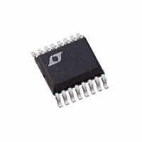
LT6300IGN#PBF Linear Technology, LT6300IGN#PBF Datasheet - Page 3

LT6300IGN#PBF
Manufacturer Part Number
LT6300IGN#PBF
Description
IC XDSL LINE DRIVER 16-SSOP
Manufacturer
Linear Technology
Type
Line Driver, Transmitterr
Datasheet
1.LT6300CGNPBF.pdf
(16 pages)
Specifications of LT6300IGN#PBF
Number Of Drivers/receivers
2/0
Protocol
xDSL
Voltage - Supply
5 V ~ 12 V
Mounting Type
Surface Mount
Package / Case
16-SSOP
Lead Free Status / RoHS Status
Lead free / RoHS Compliant
Available stocks
Company
Part Number
Manufacturer
Quantity
Price
ELECTRICAL CHARACTERISTICS
The
V
SYMBOL
A
V
I
I
SR
HD2
HD3
GBW
Note 1: Absolute Maximum Ratings are those values beyond which the life
of a device may be impaired.
Note 2: Applies to short circuits to ground only. A short circuit between
the output and either supply may permanently damage the part when
operated on supplies greater than 10V.
Note 3: The LT6300C is guaranteed to meet specified performance from
0 C to 70 C and is designed, characterized and expected to meet these
extended temperature limits, but is not tested at – 40 C and 85 C. The
LT6300I is guaranteed to meet the extended temperature limits.
OUT
S
VOL
OUT
CM
= 0V, pulse tested, 5V V
denotes the specifications which apply over the full specified temperature range, otherwise specifications are at T
PARAMETER
Large-Signal Voltage Gain
Output Swing
Maximum Output Current
Supply Current per Amplifier
Supply Current in Shutdown
Output Leakage in Shutdown
Channel Separation
Slew Rate
Differential 2nd Harmonic Distortion
Differential 3rd Harmonic Distortion
Gain Bandwidth
S
12V, V
SHDNREF
CONDITIONS
V
V
V
V
V
V
V
V
V
V
V
V
V
V
V
V
V
V
V
f = 1MHz
= 0V, R
S
S
S
S
S
S
S
S
S
S
S
S
SHDN
SHDN
S
S
S
S
S
= 12V, V
= 5V, V
= 12V, R
= 12V, I
= 5V, R
= 5V, I
= 12V, R
= 12V, R
= 12V, R
= 12V, R
= 12V, R
= 5V, R
= 12V, V
= 12V, A
= 5V, A
= 12V, A
= 12V, A
= 0.4V
= 0.4V
BIAS
L
OUT
L
BIAS
V
L
= 250mA
OUT
OUT
V
V
V
L
L
BIAS
BIAS
BIAS
BIAS
= 24.9k between V
= 25
= –10, (Note 7)
= 250mA
= – 10, (Note 7)
= 10, 2V
= 10, 2V
= 100
= 1
= 3V, R
= 24.9k (Note 6)
= 10V, R
= 10V, R
= 24.9k (Note 6)
= 32.4k (Note 6)
= 43.2k (Note 6)
= 66.5k (Note 6)
Note 4: Thermal resistance varies depending upon the amount of PC board
metal attached to Pins 1, 8, 9, 16 of the device. If the maximum
dissipation of the package is exceeded, the device will go into thermal
shutdown and be protected.
Note 5: Guaranteed by the CMRR tests.
Note 6: R
SHDNREF pin grounded.
Note 7: Slew rate is measured at 5V on a 10V output signal while
operating on 12V supplies and 1V on a 3V output signal while
operating on 5V supplies.
P-P
P-P
L
, R
, R
= 25
L
L
= 40
= 40
L
L
BIAS
= 50 , 1MHz
= 50 , 1MHz
is connected between V
+
and SHDN unless otherwise noted. (Note 3)
MIN
10.7
10.5
10.4
10.2
500
300
100
3.5
3.3
3.4
3.2
8.0
6.7
2.2
1.8
63
57
60
54
80
77
+
and the SHDN pin, with the
1200
10.9
10.7
TYP
– 85
– 82
110
600
200
200
3.8
3.7
3.4
0.1
0.3
70
10
76
8
6
4
MAX
13.5
15.0
5.0
5.8
1
1
LT6300
A
= 25 C.
UNITS
3
V/ s
V/ s
MHz
dBc
dBc
mA
mA
mA
mA
mA
mA
mA
mA
mA
mA
dB
dB
dB
dB
dB
dB
V
V
V
V
V
V
V
V


