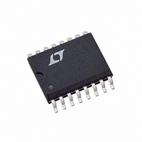
LTC487CSW Linear Technology, LTC487CSW Datasheet - Page 5

LTC487CSW
Manufacturer Part Number
LTC487CSW
Description
IC DVR RS485 LOW PWR QUAD 16SOIC
Manufacturer
Linear Technology
Type
Driverr
Datasheet
1.LTC487CNPBF.pdf
(12 pages)
Specifications of LTC487CSW
Number Of Drivers/receivers
4/0
Protocol
RS422, RS485
Voltage - Supply
4.75 V ~ 5.25 V
Mounting Type
Surface Mount
Package / Case
16-SOIC (0.300", 7.5mm Width)
Lead Free Status / RoHS Status
Contains lead / RoHS non-compliant
Other names
LTC487CS
Available stocks
Company
Part Number
Manufacturer
Quantity
Price
Part Number:
LTC487CSW
Manufacturer:
LINEAR
Quantity:
20 000
Company:
Part Number:
LTC487CSW#PBF
Manufacturer:
Maxim
Quantity:
150
Part Number:
LTC487CSW#PBF
Manufacturer:
LINEAR/凌特
Quantity:
20 000
Part Number:
LTC487CSW#TRPBF
Manufacturer:
LTNEAR
Quantity:
20 000
pin FuncTions
DI1 (Pin 1): Driver 1 Input. If Driver 1 is enabled, then a
low on DI1 forces the driver outputs DO1A low and DO1B
high. A high on DI1 with the driver outputs enabled will
force DO1A high and DO1B low.
DO1A (Pin 2): Driver 1 Output.
DO1B (Pin 3): Driver 1 Output.
EN12 (Pin 4): Driver 1 and 2 Outputs Enabled. See Func-
tion Table for details.
DO2B (Pin 5): Driver 2 Output.
DO2A (Pin 6): Driver 2 Output.
DI2 (Pin 7): Driver 2 Input. Refer to DI1.
FuncTion Table
swiTching TiMe waveForMs
EN12
A, B
DI
A, B
–V
V
3V
0V
V
V
3V
0V
5V
0V
OL
OH
B
A
O
INPUT
O
DI
H
X
L
V
O
EN12 or EN34
ENABLES
H
H
L
1/2 V
O
10%
t
r
t
PLH
OUT A
1.5V
1.5V
t
t
ZH
ZL
80%
H
L
Z
2.3V
2.3V
OUTPUTS
t
Figure 2. Driver Enable and Disable Times
SKEW
Figure 1. Driver Propagation Delays
OUT B
L
H
Z
f = 1MHz : t
f = 1MHz : t
OUTPUT NORMALLY HIGH
OUTPUT NORMALLY LOW
V
DIFF
r
= V(A) – V(B)
r
<
≤
10ns : t
10ns : t
GND (Pin 8): GND Connection.
DI3 (Pin 9): Driver 3 Input. Refer to DI1.
DO3A (Pin 10): Driver 3 Output.
DO3B (Pin 11): Driver 3 Output.
EN34 (Pin 12): Driver 3 and 4 Outputs Enabled. See Func-
tion Table for details.
DO4B (Pin 13): Driver 4 Output.
DO4A (Pin 14): Driver 4 Output.
DI4 (Pin 15): Driver 4 Input. Refer to DI1.
V
H: High Level
L: Low Level
X: Irrelevant
Z: High Impedance (Off)
CC
f
(Pin 16): Positive Supply; 4.75 < V
f
<
≤
10ns
10ns
1/2 V
O
t
t
t
HZ
LZ
PHL
1.5V
1.5V
t
90%
f
20%
t
0.5V
0.5V
SKEW
CC
LTC487
< 5.25.
LTC487 • TA05
LTC487 • TA06
487fc


