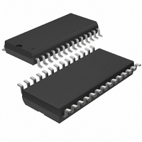
LTC1348CSW Linear Technology, LTC1348CSW Datasheet - Page 6

LTC1348CSW
Manufacturer Part Number
LTC1348CSW
Description
IC TXRX 3.3V/5V RS232 28-SOIC
Manufacturer
Linear Technology
Type
Transceiverr
Datasheet
1.LTC1348CSWPBF.pdf
(8 pages)
Specifications of LTC1348CSW
Number Of Drivers/receivers
3/5
Protocol
RS232
Voltage - Supply
3 V ~ 5.5 V
Mounting Type
Surface Mount
Package / Case
28-SOIC (7.5mm Width)
Lead Free Status / RoHS Status
Contains lead / RoHS non-compliant
Other names
LTC1348CS
Available stocks
Company
Part Number
Manufacturer
Quantity
Price
Part Number:
LTC1348CSW
Manufacturer:
LT/凌特
Quantity:
20 000
Company:
Part Number:
LTC1348CSW#PBF
Manufacturer:
LTC
Quantity:
600
Part Number:
LTC1348CSW#TRPBF
Manufacturer:
LINEAR/凌特
Quantity:
20 000
SWITCHI G TI E WAVEFOR S
APPLICATIONS
LTC1348
Power Supply
The LTC1348 includes an onboard voltage-tripling charge
pump capable of generating 8V from a single 3.3V
supply. This allows the LTC1348 drivers to provide guar-
anteed 5V RS232-compliant voltage levels with a 3.3V
supply. With all outputs loaded with 3k , the LTC1348
can typically swing 5V with voltages as low as 2.85V. It
will meet the 3.7V EIA562 levels with supply voltages as
6
TEST CIRCUITS
OUTPUT
DRIVER
DRIVER
INPUT
t
LHD
Figure 1. Driver Propagation Delay Timing
1.4V
Figure 4. Receiver Timing Test Load
DRIVER
RX INPUT
U
Figure 3. Driver Timing Test Load
INPUT
0V
U
W
DRIVER
INFORMATION
RX
U
OUTPUT
DRIVER
OUTPUT
W
RX
LTC1348 • F04
51pF
51pF
1.4V
LTC1348 • F03
3k
t
HLD
U
W
0V
LTC1348 • F01
V
0V
V
V
CC
+
–
PROTECTED TO 10kV
RS232 LINE PINS
low as 2.2V. The charge pump requires three external
flying capacitors to operate; 0.1 F ceramic capacitors are
adequate for most applications. For applications requiring
extremely high data rates or abnormally heavy output
loads, 0.33 F flying capacitors are recommended. Bypass
and output capacitor values should match those of the
flying capacitors and all capacitors should be mounted as
close to the package as possible.
OUTPUT
INPUT
0.1 F
0.1 F
RX
RX
t
LHR
Figure 2. Receiver Propagation Delay Timing
0.1 F
0.1 F
DR1 OUT
DR2 OUT
DR3 OUT
V
RX1 IN
RX2 IN
RX3 IN
RX4 IN
RX5 IN
CC
V
1.7V
+
0.8V
C2
C2
C1
C1
+
–
+
–
10
11
12
13
14
1
2
3
4
5
6
7
8
9
ESD Test Circuit
LTC1348
LT1348 • TC
28
27
26
25
24
23
22
21
20
19
18
17
16
15
1.3V
C3
C3
DR1 IN
RX1 OUT
DR2 IN
RX2 OUT
RX3 OUT
RX4 OUT
DR3 IN
RX5 OUT
DREN
RXEN
GND
+
–
V
t
–
HLR
0.1 F
2.4V
LTC1348 • F02
0.1 F
V
0V
V
0V
CC
CC


