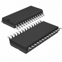
LTC1337CSW#TRPBF Linear Technology, LTC1337CSW#TRPBF Datasheet - Page 4

LTC1337CSW#TRPBF
Manufacturer Part Number
LTC1337CSW#TRPBF
Description
IC 3DVR/5RCVR 5V RS232 28-SOIC
Manufacturer
Linear Technology
Type
Transceiverr
Datasheet
1.LTC1337CGPBF.pdf
(8 pages)
Specifications of LTC1337CSW#TRPBF
Number Of Drivers/receivers
3/5
Protocol
RS232
Voltage - Supply
4.5 V ~ 5 V
Mounting Type
Surface Mount
Package / Case
28-SOIC (7.5mm Width)
Lead Free Status / RoHS Status
Lead free / RoHS Compliant
Available stocks
Company
Part Number
Manufacturer
Quantity
Price
V
the Shutdown mode. This pin should be decoupled with a
0.1µF ceramic capacitor.
GND: Ground Pin.
ON/OFF: TTL/CMOS Compatible Shutdown Pin. A logic
low puts the device in the Shutdown mode which reduces
input supply current to less than 1µA and places all drivers
and receivers in high impedance state. This pin cannot
float.
V
1V. This pin requires an external capacitor C = 0.1µF for
charge storage. The capacitor may be tied to ground or 5V.
LTC1337
4
TYPICAL PERFOR A CE CHARACTERISTICS
PI FU CTIO S
CC
+
: Positive Supply Output (RS232 Drivers). V
20
16
14
12
10
55
50
45
40
35
30
25
20
15
10
U
: 5V Input Supply Pin. Supply current less than 1µA in
8
6
4
2
0
0
0
V
Receiver Short-Circuit Current
CC
Supply Current
10
10
U
3 DRIVERS LOADED
20
20
1 DRIVER LOADED
TEMPERATURE (°C)
TEMPERATURE (°C)
R
R
30
30
L
L
I
I
= 3k
= 3k
SC
SC
U
–
+
40
40
50
50
W
60
60
1337 G04
1337 G07
U
70
70
C
L
= 2500pF
OUTPUT
OUTPUT
DRIVER
DRIVER
R
R
INPUT
L
L
= 3k
= 3k
45
40
35
30
25
20
15
10
5
0
0
Driver Output Waveforms
Driver Leakage in Shutdown
+
≅ 2V
10
CC
20
TEMPERATURE (°C)
–
30
V
With multiple devices, the V
leled into common capacitors. For large numbers of
devices, increasing the size of the shared common storage
capacitors is recommended to reduce ripple.
V
–1.5V). This pin requires an external capacitor C = 0.1µF
for charge storage.
C1
pins require two external capacitors C = 0.1µF. One from
C1
charge pump efficiency, the capacitor’s effective series
resistance should be less than 50Ω.
V
OUT
OUT
–
40
: Negative Supply Output (RS232 Drivers). V
+
+
= –20V
, C1
= 20V
to C1
50
–
, C2
–
60
1337 G05
, and another from C2
+
, C2
70
–
: Commutating Capacitor Inputs. These
C
OUTPUT
L
= 50pF
INPUT
RX
20
18
16
14
12
10
8
6
4
2
0
Driver Short-Circuit Current
Receiver Output Waveforms
+
10
and V
20
+
TEMPERATURE (°C)
–
to C2
pins may be paral-
30
I
I
SC
SC
+
–
–
40
. To maintain
50
–
≅ (2V
60
1337 G06
1337fa
CC
70


