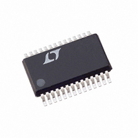
LTC1347CG Linear Technology, LTC1347CG Datasheet - Page 5

LTC1347CG
Manufacturer Part Number
LTC1347CG
Description
IC TXRX 5V RS232 LOW PWR 28-SSOP
Manufacturer
Linear Technology
Type
Transceiverr
Specifications of LTC1347CG
Number Of Drivers/receivers
3/5
Protocol
RS232
Voltage - Supply
5V
Mounting Type
Surface Mount
Package / Case
28-SSOP
Lead Free Status / RoHS Status
Contains lead / RoHS non-compliant
Available stocks
Company
Part Number
Manufacturer
Quantity
Price
Part Number:
LTC1347CG
Manufacturer:
LINEAR/凌特
Quantity:
20 000
Part Number:
LTC1347CG#TRPBF
Manufacturer:
LTNEAR
Quantity:
20 000
SWITCHI G TI E WAVEFOR S
charge pump efficiency, the capacitor’s effective series
resistance should be less than 2Ω.
DRIVER IN: RS232 Driver Input Pins. Inputs are TTL/
CMOS compatible. Inputs should not be allowed to float.
Tie unused inputs to V
DRIVER OUT: Driver Outputs at RS232 Voltage Levels.
Outputs are in a high impedance state when in Shutdown
mode or V
ESD to ±10kV for human body model discharges.
PI FU CTIO S
U
CC
U
= 0V. The driver outputs are protected against
U
U
CC
W
.
OUTPUT
OUTPUT
DRIVER
DRIVER
INPUT
INPUT
RX
RX
t
LHR
t
LHD
Figure 1. Driver Propagation Delay Timing
Figure 2. Receiver Propagation Delay Timing
1.4V
1.7V
W
0.8V
0V
RX IN: Receiver Inputs. These pins can be forced to ±25V
without damage. The receiver inputs are protected against
ESD to ±10kV for human body model discharges. Each
receiver provides 0.4V of hysteresis for noise immunity.
RX OUT: Receiver Outputs with TTL/CMOS Voltage Lev-
els. All receivers are kept alive in Shutdown.
1.4V
1.3V
t
HLD
t
HLR
0V
2.4V
1347 F01
1347 F02
V
0V
V
V
V
0V
V
0V
CC
+
–
CC
CC
LTC1347
1347fa
5


