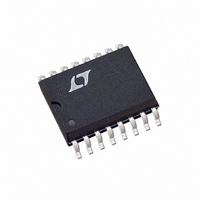
LTC1688CS Linear Technology, LTC1688CS Datasheet - Page 5

LTC1688CS
Manufacturer Part Number
LTC1688CS
Description
IC DVR 100MBPS RS485 QUAD 16SOIC
Manufacturer
Linear Technology
Type
Driverr
Datasheet
1.LTC1688CSPBF.pdf
(12 pages)
Specifications of LTC1688CS
Number Of Drivers/receivers
4/0
Protocol
RS485
Voltage - Supply
3V, 5V
Mounting Type
Surface Mount
Package / Case
16-SOIC (3.9mm Width)
Lead Free Status / RoHS Status
Contains lead / RoHS non-compliant
Available stocks
Company
Part Number
Manufacturer
Quantity
Price
Part Number:
LTC1688CS
Manufacturer:
LINEAR/凌特
Quantity:
20 000
Company:
Part Number:
LTC1688CS#PBF
Manufacturer:
LTC
Quantity:
211
DI1 (Pin 1): Driver 1 Input. Do not float.
DO1A (Pin 2): Driver 1 Noninverting Output.
DO1B (Pin 3): Driver 1 Inverting Output.
EN (Pin 4, LTC1688): High True Enable Pin, enables all
four drivers. A low on Pin 4 and a high on Pin 12 will put
all driver outputs into a high impedance state. See
Function Tables for details. Do not float.
EN12 (Pin 4, LTC1689): Enables Drivers 1 and 2. A low on
Pin 4 will put the outputs of drivers 1 and 2 into a high
impedance state. See Function Tables for details. Do not
float.
DO2B (Pin 5): Driver 2 Inverting Output.
DO2A (Pin 6): Driver 2 Noninverting Output.
DI2 (Pin 7): Driver 2 Input. Do not float.
GND (Pin 8): Ground Connection. A good ground plane is
recommended for all applications.
FU CTIO TABLES
PIN
LTC1688
TEST CIRCUITS
Figure 1. Driver DC Test Load
U
U
DI
H
H
X
B
L
L
A
FUNCTIONS
V
OD
U
INPUTS
U
R
R
EN
H
H
X
X
L
1688/89 TC01
V
OC
U
ENB
X
X
H
L
L
OUTA
HI-Z
H
H
DI
L
L
Figure 2. Driver Timing Test Circuit
OUTPUTS
ENB (EN34)
EN (EN12)
DRIVER
OUTB
HI-Z
H
H
L
L
A
B
R
DIFF
DI3 (Pin 9): Driver 3 Input. Do not float.
DO3A (Pin 10): Driver 3 Noninverting Output.
DO3B (Pin 11): Driver 3 Inverting Output.
ENB (Pin 12, LTC1688): Low True Enable Pin, enables all
four drivers. A low on Pin 4 and a high on Pin 12 will put
all driver outputs into a high impedance state. See
Function Tables for details. Do not float.
EN34 (Pin 12, LTC1689): Enables Drivers 3 and 4. A low
on Pin 12 will put the outputs of drivers 3 and 4 into a high
impedance state. See Function Tables for details. Do not
float.
DO4B (Pin 13): Driver 4 Inverting Output.
DO4A (Pin 14): Driver 4 Noninverting Output.
DI4 (Pin 15): Driver 4 Input. Do not float.
V
bypassed with a 0.1 F ceramic capacitor as close to the
pin as possible. Recommended: V
LTC1689
DD
C
C
L1
L2
1688/89 TC02
(Pin 16): Power Supply Input. This pin should be
DI
H
L
X
INPUTS
UNDER TEST
EN12/EN34
OUTPUT
Figure 3. Driver Timing Test Load
H
H
LTC1688/LTC1689
L
500
C
L
DD
OUTA
HI-Z
= 3V to 5.25V.
H
L
OUTPUTS
S1
S2
OUTB
HI-Z
1688/89 TC03
H
L
16889fa
5
V
DD


