LTC1520CS Linear Technology, LTC1520CS Datasheet - Page 2
LTC1520CS
Manufacturer Part Number
LTC1520CS
Description
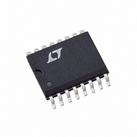
IC LINE RCVR HI-SPD QUAD 16-SOIC
Manufacturer
Linear Technology
Type
Line Receiverr
Datasheet
1.LTC1520CSPBF.pdf
(8 pages)
Specifications of LTC1520CS
Number Of Drivers/receivers
0/4
Protocol
LVDS
Voltage - Supply
4.75 V ~ 5.25 V
Mounting Type
Surface Mount
Package / Case
16-SOIC (3.9mm Width)
Lead Free Status / RoHS Status
Contains lead / RoHS non-compliant
Available stocks
Company
Part Number
Manufacturer
Quantity
Price

Part Number:
LTC1520CS
Manufacturer:
LINEAR/凌特
Quantity:
20 000
Part Number:
LTC1520CS#PBF
Manufacturer:
LINEAR/凌特
Quantity:
20 000


A
(Note 1)
Supply Voltage ....................................................... 10V
Digital Input Currents ..................... – 100mA to 100mA
Digital Input Voltages ............................... – 0.5V to 10V
Receiver Input Voltages ........................................ 10V
Receiver Output Voltages ............. – 0.5V to V
Short-Circuit Duration .................................... Indefinite
Operating Temperature Range .................... 0 C to 70 C
Storage Temperature Range ................ – 65 C to 150 C
Lead Temperature (Soldering, 10 sec)................. 300 C
DC ELECTRICAL CHARACTERISTICS
LTC1520
V
SYMBOL
V
V
V
I
I
R
C
V
V
dV
V
V
I
I
I
CMRR
2
IN1
IN2
OZR
DD
OSR
CM
IH
IL
IN
OC
ID(MIN)
OH
OL
DD
IN
BSOLUTE
ID
= 5V 5% (Notes 2, 3) per receiver, unless otherwise noted.
PARAMETER
Input Common Mode Voltage
Input High Voltage
Input Low Voltage
Input Current
Input Current (A, B)
Input Resistance (Figure 5)
A, B Input Capacitance
Open-Circuit Input Voltage (Figure 5)
Differential Input Threshold Voltage
Input Hysteresis
Output High Voltage
Output Low Voltage
Three-State Output Current
Total Supply Current All 4 Receivers
Short-Circuit Current
Common Mode Rejection Ratio
W
A
XI
W
U
W
R
A
TI
CONDITIONS
A, B Inputs
Enable Input
Enable Input
Enable Input
V
V
– 0.2V V
(Note 4)
V
– 0.2V < V
V
I
I
0V V
V
V
V
OUT
OUT
U
A
A
DD
CM
ID
OUT
CM
, V
, V
DD
G
= 5V (Note 4)
= 2.5V
= 2.5V, f = 25MHz
= – 4mA, V
= 4mA, V
B
B
= 0V, V
0.1V, No Load, Enable = 5V
OUT
= 5V
= 0
+ 0.5V
S
CM
CM
OUT
V
< V
ID
DD
V
ID
= 0.1V, V
DD
DD
= V
= 0.1V, V
+ 0.2V
+ 0.2V
DD
PACKAGE/ORDER I FOR ATIO
Consult factory for Industrial and Military grade parts.
DD
ENABLE
DD
OUT 1
OUT 2
= 5V
GND
= 5V
B1
A1
A2
B2
T
JMAX
1
2
3
4
5
6
7
8
16-LEAD PLASTIC SO
= 150 C,
S PACKAGE
TOP VIEW
JA
= 90 C/ W
– 250
– 0.2
– 0.1
16
15
14
13
12
11
10
MIN
– 10
– 50
9
3.2
4.6
– 1
18
2
V
B4
A4
OUT 4
NC
OUT 3
A3
B3
DD
U
TYP
3.3
20
12
45
3
ORDER PART
V
LTC1520CS
DD
W
NUMBER
MAX
250
0.8
3.4
0.1
0.4
10
20
50
1
+ 0.2
UNITS
U
mV
mA
mA
k
dB
pF
V
V
V
A
A
A
V
V
V
V
A
Related parts for LTC1520CS
Image
Part Number
Description
Manufacturer
Datasheet
Request
R

Part Number:
Description:
CD ROM LINEARVIEW DATASHEETS
Manufacturer:
Linear Technology

Part Number:
Description:
Standalone Linear Li-Ion Battery Charger with Thermal Regulation in ThinSOT
Manufacturer:
Linear Technology Corporation
Datasheet:
Part Number:
Description:
Low noise, high frequency, 8th order linear phase lowpass filter
Manufacturer:
Linear Technology Corporation
Datasheet:
Part Number:
Description:
Manufacturer:
Linear Technology Corporation
Datasheet:
Part Number:
Description:
Manufacturer:
Linear Technology Corporation
Datasheet:
Part Number:
Description:
Manufacturer:
Linear Technology Corporation
Datasheet:
Part Number:
Description:
Manufacturer:
Linear Technology Corporation
Datasheet:
Part Number:
Description:
Manufacturer:
Linear Technology Corporation
Datasheet:
Part Number:
Description:
Manufacturer:
Linear Technology Corporation
Datasheet:
Part Number:
Description:
Manufacturer:
Linear Technology Corporation
Datasheet:
Part Number:
Description:
Dual and Quad, JFET Input Precision High Speed Op Amps
Manufacturer:
Linear Technology Corporation
Datasheet:
Part Number:
Description:
Manufacturer:
Linear Technology Corporation
Datasheet:
Part Number:
Description:
1, 2, 6 and 8 Channel, 10-Bit Serial I/O Data Acquisition Systems
Manufacturer:
Linear Technology Corporation
Datasheet:
Part Number:
Description:
Manufacturer:
Linear Technology Corporation
Datasheet:
Part Number:
Description:
Universal dual filter building block
Manufacturer:
Linear Technology Corporation
Datasheet: