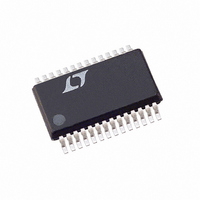
LTC1348IG#TR Linear Technology, LTC1348IG#TR Datasheet - Page 5

LTC1348IG#TR
Manufacturer Part Number
LTC1348IG#TR
Description
IC TXRX RS232 3.3-5V LPWR 28SSOP
Manufacturer
Linear Technology
Type
Transceiverr
Datasheet
1.LTC1348CSWPBF.pdf
(8 pages)
Specifications of LTC1348IG#TR
Number Of Drivers/receivers
3/5
Protocol
RS232
Voltage - Supply
3 V ~ 5.5 V
Mounting Type
Surface Mount
Package / Case
28-SSOP
Lead Free Status / RoHS Status
Contains lead / RoHS non-compliant
Available stocks
Company
Part Number
Manufacturer
Quantity
Price
PI FU CTIO S
V
decoupled with a 0.1 F ceramic capacitor.
GND: Ground Pin.
RXEN: TTL/CMOS Compatible Enable Pin. Refer to Table
1 for its functional description.
DREN: TTL/CMOS Compatible Enable Pin. Refer to Table
1 for its functional description.
V
requires an external capacitor C = 0.1 F for charge stor-
age. The capacitor may be tied to ground or V
multiple devices, the V
common capacitors. For large numbers of devices, in-
creasing the size of the shared common storage capaci-
tors is recommended to reduce ripple.
V
requires an external capacitor C = 0.1 F for charge
storage.
C1
Inputs. These pins require three external capacitors C =
0.1 F: one from C1
another from C3
Table 1. Functional Description
MODE
Shutdown
Receiver
Disable
Receiver
Alive
Normal
CC
+
–
: Positive Supply Output (RS232 Drivers). This pin
: Negative Supply Output (RS232 Drivers). This pin
+
U
: 3V to 5.5V Input Supply Pin. This pin should be
, C1
–
, C2
U
RX ENABLE
+
, C2
0
0
1
1
+
–
+
, C3
to C3
to C1
U
+
and V
DR ENABLE
+
, C3
–
–
, another from C2
. To maintain charge pump
0
1
0
1
–
–
pins may be paralleled into
: Commutating Capacitor
DRIVERS
All Drivers Shutdown.
All Driver Outputs Assume High Impedance.
All Driver Pull-Up Resistors Disconnect
From V
All Drivers Alive.
All Drivers Shutdown.
All Driver Outputs in Three-State.
All Driver Pull-Up Resistors Disconnect
From V
All Drivers Alive.
CC
CC
.
.
+
to C2
CC
. With
–
and
efficiency, the capacitor’s effective series resistance should
be less than 1 . Ceramic capacitors are recommended.
DR IN: RS232 Driver Input Pins. Inputs are TTL/CMOS
compatible. The inputs of unused drivers can be left
unconnected since 300k input pull-up resistors to V
included on chip. To minimize power consumption, the
internal driver pull-up resistors are disconnected from V
in the Shutdown or Receiver Alive mode.
DR OUT: Driver Outputs at RS232 Voltage Levels. Outputs
are in a high impedance state when in the Shutdown,
Receiver Alive mode or V
protected against ESD to 10kV for human body model
discharges.
RX IN: Receiver Inputs. These pins can be forced to 25V
without damage. The receiver inputs are protected against
ESD to 10kV for human body model discharges. Each
receiver provides 0.4V of hysteresis for noise immunity. In
Receiver Alive mode all receivers have no hysteresis.
RX OUT: Receiver Outputs with TTL/CMOS Voltage Lev-
els. Outputs are in a high impedance state when in the
Shutdown or Receiver Disable mode to allow data line
sharing.
RECEIVERS
All Receivers Shutdown.
All Receiver Outputs Assume High Impedance.
All Receiver Outputs in Three-State.
All Receivers Alive.
All Receivers Alive.
CC
= 0V. The driver outputs are
LTC1348
600 A at
800 A at
600 A at
800 A at
CC
I
CC
0.2 A
3.3V,
15 A
3.3V,
5
are
TYP
CC
5V
5V


