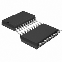
LT1794ISW#TR Linear Technology, LT1794ISW#TR Datasheet - Page 14

LT1794ISW#TR
Manufacturer Part Number
LT1794ISW#TR
Description
IC OPAMP 200MHZ DUAL 20-SOIC
Manufacturer
Linear Technology
Type
Line Driver, Transmitterr
Datasheet
1.LT1794CSWPBF.pdf
(20 pages)
Specifications of LT1794ISW#TR
Number Of Drivers/receivers
2/0
Protocol
xDSL
Voltage - Supply
18V
Mounting Type
Surface Mount
Package / Case
20-SOIC (7.5mm Width)
Lead Free Status / RoHS Status
Contains lead / RoHS non-compliant
Other names
LT1794ISWTR
Available stocks
Company
Part Number
Manufacturer
Quantity
Price
LT1794
APPLICATIO S I FOR ATIO
In differential driver applications, as shown on the first
page of this data sheet, it is recommended that the gain
setting resistor be comprised of two equal value resistors
connected to a good AC ground at high frequencies. This
ensures that the feedback factor of each amplifier remains
less than 0.1 at any frequency. The midpoint of the
resistors can be directly connected by ground, with the
resulting DC gain to the V
bypassed to ground with a 1000pF or larger capacitor.
Line Driving Back-Termination
The standard method of cable or line back-termination is
shown in Figure 13. The cable/line is terminated in its
characteristic impedance (50 , 75 , 100 , 135 , etc.).
A back-termination resistor also equal to the chararacteristic
impedance should be used for maximum pulse fidelity of
outgoing signals, and to terminate the line for incoming
signals in a full-duplex application. There are three main
drawbacks to this approach. First, the power dissipated in
the load and back-termination resistors is equal so half of
the power delivered by the amplifier is wasted in the
termination resistor. Second, the signal is halved so the
gain of the amplifer must be doubled to have the same
overall gain to the load. The increase in gain increases
noise and decreases bandwidth (which can also increase
distortion). Third, the output swing of the amplifier is
doubled which can limit the power it can deliver to the load
for a given power supply voltage.
An alternate method of back-termination is shown in
Figure 14. Positive feedback increases the effective back-
termination resistance so R
14
C
V
BIG
C
I
C
R
R
G
C
Figure 12. Combination Compensation
+
–
R
F
U
U
BT
OS
V
V
V
O
O
I
can be reduced by a factor
= 1 AT LOW FREQUENCIES
= 1 +
= 1 +
of the amplifiers, or just
R
(R
R
W
G
F
C
R
AT MEDIUM FREQUENCIES
|| R
F
G
)
AT HIGH FREQUENCIES
U
1794 F12
of n. To analyze this circuit, first ground the input. As R
R
Eliminating V
For example, reducing R
amplifer gain of (1 + R
= 12.3.
L
/n, and assuming R
V
R
V
V
(1 + R
A
P
O
BT
Figure 14. Back Termination Using Postive Feedback
= V
= V
= V
Figure 13. Standard Cable/Line Back Termination
R
by n.
V
G
V
I
I
P2
O
P
O
(1 – 1/n)/(1 + R
(1 + R
/R
(1 – 1/n) to increase the effective value of
R
+
–
P1
P
P1
R
, we get the following:
G
) = (1 + R
V
P2
R
P
F
/R
+
–
P1
P2
FOR R
V
V
1 +
O
I
F
BT
)
/R
>>R
R
=
F
F
R
R
/R
CHARACTERISTIC IMPEDANCE R
BT
G
by a factor of n = 4, and with an
G
F
F
R
R
1 +
/R
) = 10 requires that R
1 + 1/n
=
G
BT
L
R
P2
R
P1
R
)/(1 – 1/n)
R
n
V
V
we require that:
G
CABLE OR LINE WITH
R
L
R
R
P2
BT
O
I
G
+ R
F
)
P1
/(R
=
= R
V
P2
1
2
–
P2
A
L
(1 + R
R
+ R
= 1 –
P2
R
R
BT
P1
+ R
P1
F
)
/R
1
n
R
P1
L
G
V
R
)
O
L
1794 F14
1794 F13
L
V
O
P2
/R
BT
P1
=


