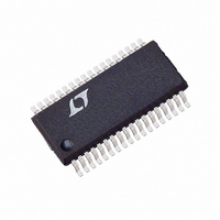
LTC1545CG#TR Linear Technology, LTC1545CG#TR Datasheet - Page 12

LTC1545CG#TR
Manufacturer Part Number
LTC1545CG#TR
Description
IC TXRX SOFTWARE SELECTBL 36SSOP
Manufacturer
Linear Technology
Type
Transceiverr
Datasheet
1.LTC1545CGTR.pdf
(16 pages)
Specifications of LTC1545CG#TR
Number Of Drivers/receivers
5/5
Voltage - Supply
4.75 V ~ 5.25 V
Mounting Type
Surface Mount
Package / Case
36-SSOP
Lead Free Status / RoHS Status
Contains lead / RoHS non-compliant
Protocol
-
Available stocks
Company
Part Number
Manufacturer
Quantity
Price
APPLICATIONS
LTC1545
Any mismatch in the driver rise and fall times or skew in
the driver propagation delays will force current through
the center termination resistor to ground, causing a high
frequency common mode spike on the A and B terminals.
The common mode spike can cause EMI problems that are
reduced by capacitor C1 which shunts much of the com-
mon mode energy to ground rather than down the cable.
No-Cable Mode
The no-cable mode (M0 = M1 = M2 = D4ENB = 1, R4EN = 0)
is intended for the case when the cable is disconnected
from the connector. The charge pump, bias circuitry,
drivers and receivers are turned off, the driver outputs are
forced into a high impedance state, and the supply current
drops to less than 200 A.
Charge Pump
The LTC1543 uses an internal capacitive charge pump to
generate V
doubler generates about 8V on V
generates about – 7.5V for V
tantalum or ceramic capacitors are required for C1, C2, C3
and C4. The V
3.3 F. All capacitors are 16V and should be placed as close
as possible to the LTC1543 to reduce EMI. The turn-on
time for the charge pump is 60ms.
Receiver Fail-Safe
All LTC1543/LTC1545 receivers feature fail-safe opera-
tion in all modes. If the receiver inputs are left floating or
shorted together by a termination resistor, the receiver
output will always be forced to a logic high.
12
5V
C3
1 F
DD
and V
EE
C1
1 F
C4
1 F
capacitor C5 should be a minimum of
Figure 21. Charge Pump
3
2
1
4
U
EE
V
C1
C1
V
DD
CC
+
–
as shown in Figure 21. A voltage
INFORMATION
LTC1543
U
EE
. Four 1 F surface mounted
GND
DD
C2
C2
V
EE
+
–
W
and a voltage inverter
28
27
26
25
+
C2
1 F
1545 F21
C5
3.3 F
U
DTE vs DCE Operation
The DCE/DTE pin acts as an enable for Driver 3/Receiver
1 in the LTC1543, and Driver 3/Receiver 1 in the LTC1545.
The LTC1543/LTC1545 can be configured for either DTE
or DCE operation in one of two ways: a dedicated DTE or
DCE port with a connector of appropriate gender, or a port
with one connector that can be configured for DTE or DCE
operation by rerouting the signals to the LTC1543/LTC1545
using a dedicated DTE cable or dedicated DCE cable.
A dedicated DTE port using a DB-25 male connector is
shown in Figure 22. The interface mode is selected by logic
outputs from the controller or from jumpers to either V
or GND on the mode select pins. A dedicated DCE port
using a DB-25 female connector is shown in Figure 23.
A port with one DB-25 connector, can be configured for
either DTE or DCE operation is shown in Figure 24. The
configuration requires separate cables for proper signal
routing in DTE or DCE operation. For example, in DTE
mode, the TXD signal is routed to Pins 2 and 14 via Driver
1 in the LTC1543. In DCE mode, Driver 1 now routes the
RXD signal to Pins 2 and 14.
Compliance Testing
A European standard EN 45001 test report is available for
the LTC1343/LTC1545/LTC1344A chipset. A copy of the
test report is available from LTC or TUV Telecom Services
Inc. (formerly Detecon Inc.)
The title of the report is:
Test Report No. NET2/071601/98.
The address of TUV Telecom Services Inc. is:
TUV Telecom Services Inc.
Suite 107
1775 Old Highway 8
St. Paul, MN 55112 USA
Tel. +1 (612) 639-0775
Fax. +1 (612) 639-0873
CC


