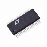
LTC2846IG#PBF Linear Technology, LTC2846IG#PBF Datasheet - Page 3

LTC2846IG#PBF
Manufacturer Part Number
LTC2846IG#PBF
Description
IC TXRX 3.3V MULTIPROTCOL 36SSOP
Manufacturer
Linear Technology
Type
Transceiverr
Datasheet
1.LTC2846CGPBF.pdf
(24 pages)
Specifications of LTC2846IG#PBF
Number Of Drivers/receivers
3/3
Protocol
Multiprotocol
Voltage - Supply
3.3V
Mounting Type
Surface Mount
Package / Case
36-SSOP
Interface Circuit Standard 1
RS-232
Number Of Receivers
3
Number Of Transmitters
3
Number Of Transceivers
1
Single Supply Voltage (typ)
3.3V
Single Supply Voltage (min)
3V
Single Supply Voltage (max)
3.6V
Dual Supply Voltage (typ)
Not RequiredV
Dual Supply Voltage (min)
Not RequiredV
Dual Supply Voltage (max)
Not RequiredV
Supply Current
170mA
Power Supply Requirement
Single
Operating Temp Range
-40C to 85C
Operating Temperature Classification
Industrial
Mounting
Surface Mount
Pin Count
36
Package Type
SSOP
Lead Free Status / RoHS Status
Lead free / RoHS Compliant
Available stocks
Company
Part Number
Manufacturer
Quantity
Price
ELECTRICAL CHARACTERISTICS
SYMBOL
V
f
t
Logic Inputs and Outputs
V
V
I
V
V
I
I
V.11 Driver
V
V
V
I
I
t
t
t
t
temperature range, otherwise specifications are at T
OSC
r
IN
OSR
OZR
SS
OZ
r
PLH
PHL
SKEW
IH
IL
OH
OL
ODO
ODL
OC
V
V
, t
t
–
OD
OC
f
PARAMETER
Negative Charge Pump Output Voltage
Charge Pump Oscillator Frequency
Charge Pump Rise Time
Logic Input High Voltage
Logic Input Low Voltage
Logic Input Current
Output High Voltage
Output Low Voltage
Output Short-Circuit Current
Three-State Output Current
Open Circuit Differential Output Voltage
Loaded Differential Output Voltage
Change in Magnitude of Differential
Output Voltage
Common Mode Output Voltage
Change in Magnitude of Common Mode
Output Voltage
Short-Circuit Current
Output Leakage Current
Rise or Fall Time
Input to Output Rising
Input to Output Falling
Input to Output Difference, t
Output to Output Skew
PLH
– t
PHL
CONDITIONS
V.28 Mode, No Load
V.28 Mode, Full Load
V.35 Mode
RS530, RS530-A, X.21 Modes, Full Load
No-Cable Mode/Power-Off to Normal Operation
D1, D2, D3, M0, M1, M2, DCE/DTE
SHDN
D1, D2, D3, M0, M1, M2, DCE/DTE
SHDN
D1, D2, D3
M0, M1, M2, DCE/DTE = GND
M0, M1, M2, DCE/DTE = V
SHDN = GND
SHDN = 3V
I
I
0V V
M0 = M1 = M2 = V
M0 = M1 = M2 = V
R
R
R
R
R
R
V
No-Cable Mode or Driver Disabled
(Figures 2, 13)
(Figures 2, 13)
(Figures 2, 13)
(Figures 2, 13)
(Figures 2, 13)
O
O
V
L
L
L
L
L
L
OUT
= – 3mA
= 1.6mA
A
A
= 1.95k (Figure 1)
= 50 (Figure 1)
= 50 (Figure 1)
= 50 (Figure 1)
= 50 (Figure 1)
= 50 (Figure 1)
= 25 C. V
= GND
and V
O
The
V
IN
B
CC
denotes specifications which apply over the full operating
0.25V, Power Off or
IN
IN
= 5V, V
, V
, V
O
O
= GND
= V
IN
IN
IN
= 3.3V, V
SHDN
= V
IN
, unless otherwise noted. (Notes 2, 3)
0.5V
– 7.5
– 5.5
– 4.5
MIN
– 30
–30
2.0
2.4
2.7
15
15
2
0
2
ODO
– 9.6
– 8.5
– 6.5
– 6.0
TYP
500
– 75
–85
0.2
16
15
40
40
2
3
3
3
1
0.67V
LTC2846
– 120
–160
MAX
0.8
0.5
0.4
0.2
0.2
32
25
65
65
12
150
100
0.1
10
10
50
10
3
5
ODO
sn2846 2846fs
UNITS
3
kHz
mA
mA
ms
ns
ns
ns
ns
ns
V
V
V
V
V
V
V
V
A
A
A
A
A
V
V
A
A
V
V
V
V
V
V
A


