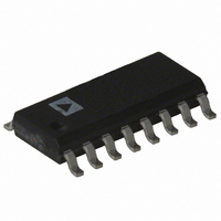
ADM202EARNZ Analog Devices Inc, ADM202EARNZ Datasheet - Page 7

ADM202EARNZ
Manufacturer Part Number
ADM202EARNZ
Description
IC TXRX RS-232 5V 15KV 16SOIC
Manufacturer
Analog Devices Inc
Type
Transceiverr
Datasheet
1.ADM202EARNZ-REEL7.pdf
(16 pages)
Specifications of ADM202EARNZ
Number Of Drivers/receivers
2/2
Protocol
RS232
Voltage - Supply
4.5 V ~ 5.5 V
Mounting Type
Surface Mount
Package / Case
16-SOIC (3.9mm Width)
Device Type
Transceiver
Ic Interface Type
RS232
No. Of Drivers
2
Supply Voltage Range
4.5V To 5.5V
Driver Case Style
SOIC
No. Of Pins
16
Operating Temperature Range
-40°C To +85°C
Lead Free Status / RoHS Status
Lead free / RoHS Compliant
Lead Free Status / RoHS Status
Lead free / RoHS Compliant, Lead free / RoHS Compliant
Available stocks
Company
Part Number
Manufacturer
Quantity
Price
Part Number:
ADM202EARNZ
Manufacturer:
ADI/亚德诺
Quantity:
20 000
Part Number:
ADM202EARNZ-REE
Manufacturer:
ADI/亚德诺
Quantity:
20 000
Company:
Part Number:
ADM202EARNZ-REEL
Manufacturer:
AD
Quantity:
2 400
Part Number:
ADM202EARNZ-REEL
Manufacturer:
ADI/亚德诺
Quantity:
20 000
Part Number:
ADM202EARNZ-REEL7
Manufacturer:
ADI原装
Quantity:
20 000
ESD/EFT TRANSIENT PROTECTION SCHEME
The ADM202E/ADM1181A use protective clamping structures
on all inputs and outputs to clamp the voltage to a safe level and
dissipate the energy present in electrostatic (ESD) and electrical
fast transients (EFT) discharges. A simplified schematic of the
protection structure is shown in Figure 8 and Figure 9. Each
input and output contains two back-to-back high speed
clamping diodes. During normal operation with maximum
RS-232 signal levels, the diodes have no effect because one or
the other is reverse biased depending on the polarity of the signal.
However, if the voltage exceeds about 50 V in either direction,
reverse breakdown occurs and the voltage is clamped at this level.
The diodes are large p-n junctions that are designed to handle
instantaneous current surges that exceed several amperes.
The transmitter outputs and receiver inputs have a similar
protection structure. The receiver inputs can dissipate some of
the energy through the internal 5 kΩ resistor to GND, as well as
through the protection diodes.
The protection structure achieves ESD protection up to ±15 kV
and EFT protection up to ±2 kV on all RS-232 I/O lines. The
methods used to test the protection scheme are discussed in the
ESD Testing (IEC1000-4-2) and Fast Transient/Burst Testing
(IEC1000-4-4) sections.
Rev. C | Page 7 of 16
RECEIVER
INPUT
Figure 9. Transmitter Output Protection Scheme
Figure 8. Receiver Input Protection Scheme
R
X
R1
D2
D1
R
T
ADM202E/ADM1181A
OUT
IN
D2
D1
TRANSMITTER
OUTPUT
R
X


