ADM5170JP Analog Devices Inc, ADM5170JP Datasheet - Page 4
ADM5170JP
Manufacturer Part Number
ADM5170JP
Description
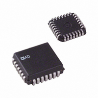
IC TXRX RS232/423 OCTAL 28PLCC
Manufacturer
Analog Devices Inc
Type
Transceiverr
Datasheet
1.ADM5170JP-REEL.pdf
(6 pages)
Specifications of ADM5170JP
Rohs Status
RoHS non-compliant
Number Of Drivers/receivers
8/8
Protocol
RS232, RS423
Voltage - Supply
9 V ~ 15 V
Mounting Type
Surface Mount
Package / Case
28-LCC (J-Lead)
Available stocks
Company
Part Number
Manufacturer
Quantity
Price
Company:

Part Number:
ADM5170JP
Manufacturer:
AD
Quantity:
5 510
Company:
Part Number:
ADM5170JP
Manufacturer:
Analog Devices Inc
Quantity:
10 000
Part Number:
ADM5170JP
Manufacturer:
ADI/亚德诺
Quantity:
20 000
Company:
Part Number:
ADM5170JP-REEL
Manufacturer:
Analog Devices Inc
Quantity:
10 000
Part Number:
ADM5170JP-REEL7
Manufacturer:
ADI/亚德诺
Quantity:
20 000
Company:
Part Number:
ADM5170JPREEL
Manufacturer:
STM
Quantity:
7 283
Part Number:
ADM5170JPZ
Manufacturer:
ADI/亚德诺
Quantity:
20 000


ADM5170
Mnemonic
V
V
GND
A
A
EN
MS+, MS–
SRA
DD
SS
I
O
. . . H
. . . H
I
O
NC = NO CONNECT
PIN FUNCTION DESCRIPTION
V
Function
Power Supply Input, +10 V
Power Supply Input, –10 V
Ground Pin. Must be connected to 0 V.
Digital Input to Drivers A to H.
RS-232/RS-423 Output from Drivers A to H.
Enable Pin. When high, all outputs are 3-stated.
Mode Select Inputs. Used to control the output
level swing. With MS+ & MS– connected to GND,
RS-423A output levels are selected. With MS+
connected to V
RS-232 output levels are developed.
Slew Rate Adjust Input. An external resistor (2 k
to 10 k ) connected between this pin and GND is
used to control the Output Slew Rate (10 V/ s to
2.2 V/ s).
B
C
D
EN
SS
C
D
O
O
O
I
I
PIN CONFIGURATIONS
10
11
SRA
7
5
8
6
9
V
NC
EN
NC
NC
A
B
C
D
SS
A
B
C
D
O
O
O
O
I
I
I
I
12
4
10
11
12
13
14
4
1
2
3
5
6
7
8
9
NC = NO CONNECT
13
3
(Not to Scale)
ADM5170
TOP VIEW
(Not to Scale)
PLCC
ADM5170
DD
14
DIP
TOP VIEW
2
and MS– connected to V
15
1
28
16
26
23
22
20
19
18
17
16
15
28
27
25
24
21
27
17
G
MS+
NC
NC
H
H
G
F
F
E
E
V
GND
26
18
MS–
I
O
I
DD
O
I
O
O
I
10%.
10%.
25
24
23
22
21
20
19
F
F
E
V
G
E
MS+
O
I
DD
I
O
O
SS
,
–4–
Slew Rate Programming
The slew rate for the ADM5170 is controlled by a single resistor
connected between the SRA pin and GND. The slew rate is
approximately.
Resistors between 2 k and 10 k may be used providing a slew
rate which may be varied from 10 V/ s to 2.2 V/ s. Figure 5 in the
Typical Performance Characteristics section shows how the slew
rate varies with R
(10% to 90%) varies with R
the user to control the level of interference (near-end crosstalk)
which may be coupled to adjacent circuits in an interconnection.
The recommended output characteristics for cable length and data
rate are given in the EIA RS-423A specifications.
Maximum Data Rate (kB/s) = 300/t (for rates from 1 kB/s to
100 kB/s).
where t is the transition time (in s) for the output to swing from
10% to 90% of its steady state values. The absolute maximum data
rate is 100 kB/s and the maximum cable length is limited to 4000 ft.
Output Mode Programming
The ADM5170 has two programmable output modes which
provide different output voltage levels. The low output mode meets
the specifications of EIA standards RS-423A while the high output
mode meets the RS-232 specifications. The high output mode
provides greater output swings and is suitable for driving lines
where higher attenuation levels must be tolerated. This mode is
selected by connecting the mode select pins to the supplies, MS+ to
V
ing both mode select pins MS+ and MS– to GND. This mode
provides a controlled output swing with lower output levels.
MS+
GND
GND
V
V
X
1
Typical Application Circuit
A typical application circuit using a single driver in the ADM5170
is shown in Figure 4. This circuit is suitable for either RS-232 or
RS-423 communication. An ADM5180 octal receiver is used to
translate the signal back to CMOS logic level at the receiving end.
Minimum Output Level.
DD
DD
DD
V
V
Figure 4. RS-232/RS-423A Typical Application Circuit
H
L
INPUT
and MS– to V
EN
Cable Length (feet) = 100 X t (Max Length = 4000 ft.)
R
SL
ADM5170
GND
GND
V
V
X
MS–
SS
SS
1/8
V
SS
V
SRA
DD
Slew Rate (V/ s) = 20/R
SS
Inputs
. The low output mode is selected by connect-
while Figure 8 shows how the transition time
0
0
EN
0
0
1
RS-232/RS-422A
TRANSMISSION
SRA
. Waveshaping of the output allows
+V
–V
0
1
Data
0
1
X
SRA
(k )
Output
5 V to 6 V (RS-423)
–5 V to –6 V (RS-423)
(V
(V
High Z
Outputs
DD
SS
TIE TO GND
FOR RS-232
+ 3 V) (RS-232)
ADM5180
– 3 V) (RS-232)
1/8
V
V
L
H
REV. 0
1
1
Related parts for ADM5170JP
Image
Part Number
Description
Manufacturer
Datasheet
Request
R

Part Number:
Description:
±1.7g Dual-Axis IMEMS Accelerometer Evaluation Board
Manufacturer:
Analog Devices Inc
Datasheet:

Part Number:
Description:
Inertial Sensor Evaluation System
Manufacturer:
Analog Devices Inc
Datasheet:
Part Number:
Description:
Manufacturer:
Analog Devices Inc
Datasheet:
Part Number:
Description:
Manufacturer:
Analog Devices Inc
Datasheet:
Part Number:
Description:
Manufacturer:
Analog Devices Inc
Datasheet:
Part Number:
Description:
Manufacturer:
Analog Devices Inc
Datasheet:
Part Number:
Description:
Manufacturer:
Analog Devices Inc
Datasheet:
Part Number:
Description:
Manufacturer:
Analog Devices Inc
Datasheet:
Part Number:
Description:
Manufacturer:
Analog Devices Inc
Datasheet:
Part Number:
Description:
Manufacturer:
Analog Devices Inc
Datasheet:
Part Number:
Description:
Manufacturer:
Analog Devices Inc
Datasheet:
Part Number:
Description:
Manufacturer:
Analog Devices Inc
Datasheet:
Part Number:
Description:
Manufacturer:
Analog Devices Inc
Datasheet: