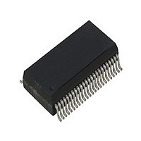
ICS1893BFI IDT, Integrated Device Technology Inc, ICS1893BFI Datasheet - Page 48

ICS1893BFI
Manufacturer Part Number
ICS1893BFI
Description
PHYCEIVER LOW PWR 3.3V 48-SSOP
Manufacturer
IDT, Integrated Device Technology Inc
Series
PHYceiver™r
Type
PHY Transceiverr
Specifications of ICS1893BFI
Protocol
MII
Voltage - Supply
3.14 V ~ 3.47 V
Mounting Type
Surface Mount
Package / Case
48-SSOP
Lead Free Status / RoHS Status
Contains lead / RoHS non-compliant
Number Of Drivers/receivers
-
Lead Free Status / Rohs Status
Not Compliant
Other names
1893BFI
Available stocks
Company
Part Number
Manufacturer
Quantity
Price
Company:
Part Number:
ICS1893BFI
Manufacturer:
OKI
Quantity:
1 934
Part Number:
ICS1893BFILF
Manufacturer:
ICS
Quantity:
20 000
6.6.2.5 Management Frame Register Address
6.6.2.6 Management Frame Operational Code
6.6.2.7 Management Frame Turnaround
6.6.2.8 Management Frame Data
6.6.2.9 Serial Management Interface Idle State
ICS1893BF, Rev. F, 5/13/10
Upon receiving a valid STA transaction, during a power-on or hardware reset an ICS1893BF compares the
PHYAD field included within the management frame with the value of its PHYAD bits stored in register 16.
(For information on the PHYAD bits, see
match its stored address bits.
A Management Frame includes a 5-bit register address field, REGAD. This field identifies which of the 32
Management Registers are involved in a transaction between an STA and a PHY.
A management frame includes a 2-bit operational code field, OP. If the operation code is a:
•
•
A valid management frame includes a turn-around field (TA), which is a 2-bit time space between the
REGAD field and the Data field. This time allows an ICS1893BF and an STA to avoid contentions during
read transactions. During an operation that is a:
•
•
A valid management frame includes a 16-bit Data field for exchanging the register contents between the
ICS1893BF and the STA. All Management Registers are 16 bits wide, matching the width of the Data field.
During a transaction that is a:
•
•
If the STA attempts to:
•
•
Note:
The MDIO signal is in an idle state during the time between STA transactions. When the Serial
Management Interface is in the idle state, the ICS1893BF disables (that is, tri-states) its MDIO pin, which
enters a high-impedance state. The ISO/IEC 8802-3 standard requires that an MDIO signal be idle for at
least one bit time between management transactions. However, the ICS1893BF does not have this
limitation and can support a continual bit stream on its MDIO signals.
Read, the REGAD field identifies the register used as the source of data returned to the STA by the
ICS1893BF.
Write, the REGAD identifies the destination register that is to receive the data sent by the STA to the
ICS1893BF.
Read, an ICS1893BF remains in the high-impedance state during the first bit time and subsequently
drives its MDIO pin to logic zero for the second bit time.
Write, an ICS1893BF waits while the STA transmits a logic one, followed by a logic zero on its MDIO pin.
Read, (OP is 10b) the ICS1893BF obtains the contents of the register identified in the REGAD field and
returns this Data to the STA synchronously with its MDC signal.
Write, (OP is 01b) the ICS1893BF stores the value of the Data field in the register identified in the
REGAD field.
Read from a non-existent ICS1893BF register, the ICS1893BF returns logic one for all bits in the Data
field, FFFFh.
Write to a non-existent ICS1893BF register, the ICS1893BF isolates the Data field of the management
frame from every reaching the registers.
ICS1893BF Data Sheet - Release
The first Data bit transmitted and received is the most-significant bit of a Management Register, bit
X.15.
Copyright © 2009, IDT, Inc.
Table
All rights reserved.
7-16.) An ICS1893BF responds to all transactions that
48
Chapter 6 Functional Blocks
May, 2010


