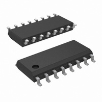
DS90LV032ATMX/NOPB National Semiconductor, DS90LV032ATMX/NOPB Datasheet - Page 7

DS90LV032ATMX/NOPB
Manufacturer Part Number
DS90LV032ATMX/NOPB
Description
IC LINE RVR 3V QUAD DIFF 16-SOIC
Manufacturer
National Semiconductor
Type
Receiverr
Datasheet
1.DS90LV032ATMTCNOPB.pdf
(12 pages)
Specifications of DS90LV032ATMX/NOPB
Number Of Drivers/receivers
0/4
Protocol
RS644
Voltage - Supply
3 V ~ 3.6 V
Mounting Type
Surface Mount
Package / Case
16-SOIC (3.9mm Width)
Lead Free Status / RoHS Status
Lead free / RoHS Compliant
Other names
*DS90LV032ATMX
*DS90LV032ATMX/NOPB
DS90LV032ATMX
*DS90LV032ATMX/NOPB
DS90LV032ATMX
Available stocks
Company
Part Number
Manufacturer
Quantity
Price
Company:
Part Number:
DS90LV032ATMX/NOPB
Manufacturer:
NS
Quantity:
22 213
Part Number:
DS90LV032ATMX/NOPB
Manufacturer:
NS/国半
Quantity:
20 000
2.
OPEN. Do not tie unused receiver inputs to ground or any
other voltages. The input is biased by internal high value
pull up and pull down resistors to set the output to a HIGH
state. This internal circuitry will guarantee a HIGH, stable
output state for open inputs.
Terminated Input. If the driver is disconnected (cable
unplugged), or if the driver is in a TRI-STATE or power-
off condition, the receiver output will again be in a HIGH
state, even with the end of cable 100Ω termination
resistor across the input pins. The unplugged cable can
become a floating antenna which can pick up noise. If the
cable picks up more than 10mV of differential noise, the
receiver may see the noise as a valid signal and switch.
To insure that any noise is seen as common-mode and
not differential, a balanced interconnect should be used.
Twisted pair cable will offer better balance than flat ribbon
cable.
Pin No.
10, 14
11, 13
9, 15
2, 6,
1, 7,
3, 5,
−40°C to +85°C
−40°C to +85°C
12
16
Temperature
4
8
Operating
FIGURE 6. ICC vs Frequency, four channels switching
Name
R
GND
R
R
EN*
V
EN
OUT
IN+
IN−
CC
Ordering Information
Pin Descriptions
Package Type/
TSSOP/MTC16
SOP/M16A
Non-inverting receiver input pin
Inverting receiver input pin
Receiver output pin
Active high enable pin, OR-ed with EN*
Active low enable pin, OR-ed with EN
Power supply pin, +3.3V ± 0.3V
Ground pin
Number
7
3.
External lower value pull up and pull down resistors (for a
stronger bias) may be used to boost fail-safe in the presence
of higher noise levels. The pull up and pull down resistors
should be in the 5kΩ to 15kΩ range to minimize loading and
waveform distortion to the driver. The common-mode bias
point should be set to approximately 1.2V (less than 1.75V)
to be compatible with the internal circuitry.
The footprint of the DS90LV032A is the same as the industry
standard 26LS32 Quad Differential (RS-422) Receiver.
Shorted Inputs. If a fault condition occurs that shorts
the receiver inputs together, thus resulting in a 0V
differential input voltage, the receiver output will remain
in a HIGH state. Shorted input fail-safe is not supported
across the common-mode range of the device (GND to
2.4V). It is only supported with inputs shorted and no
external common-mode voltage applied.
Description
10006708
DS90LV032ATMTC
DS90LV032ATM
Order Number
www.national.com


