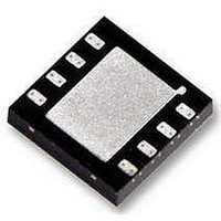
LMH6553SD National Semiconductor, LMH6553SD Datasheet - Page 18

LMH6553SD
Manufacturer Part Number
LMH6553SD
Description
DIFF AMP, 900MHZ, 8LLP, POWERWISE
Manufacturer
National Semiconductor
Datasheet
1.LMH6553SDE.pdf
(24 pages)
Specifications of LMH6553SD
No. Of Amplifiers
1
Gain Db Max
1dB
Bandwidth
900MHz
Slew Rate
2300V/µs
Supply Voltage Range
4.5V To 12V
Supply Current
29.1mA
Amplifier Case Style
LLP
No. Of Pins
8
Rohs Compliant
Yes
www.national.com
SPLIT SUPPLY OPERATION
For optimum performance, split supply operation is recom-
mended using +5V and −5V supplies; however, operation is
possible on split supplies as low as +2.25V and −2.25V and
as high as +6V and −6V. Provided the total supply voltage
does not exceed the 4.5V to 12V operating specification,
asymmetric supply operation is also possible and in some
cases advantageous. For example, if 5V DC coupled opera-
tion is required for low power dissipation but the amplifier input
common mode range prevents this operation, it is still possi-
ble
(V
input common mode voltage to suit the application.
CLAMP OPERATION
The output clamp allows control of the maximum amplifier
output swing to prevent overdriving of following stages such
as sensitive ADC inputs and provide fast recovery from signal
transients that would otherwise saturate the signal path. Fig-
ure 6 shows the relationship between V
and −OUT outputs. The example circuit shown has a single
ended input and is set for a gain of 2 V/V. For proper operation
V
voltage is limited to the voltage level set at the V
The output common mode control loop forces the lower single
ended voltage to be limited to 2*V
clamped single ended output swing is therefore equal to 2*
(V
therefore equal to 4*(V
6 with V
single ended output is therefore 1 V
the maximum differential output is 2 V
case of a 2 V
unclamped operation would provide single ended outputs at
+OUT and -OUT of 2 V
1 V
CM
+
CLAMP
) - (V
PP
< V
with
.
CLAMP
−
CLAMP
- V
) = 5V and V
CM
split
PP
< V
) and the maximum differential output swing is
set to 2V and V
FIGURE 6. Clamp Operation
input sine wave which for a gain of 2 V/V in
CM
supplies
+ 2.0V and the upper single ended output
+
and V
CLAMP
PP
but is shown being clamp limited to
−
- V
of
are selected to set the amplifier
CM
CM
CM
(V
set to 1.5V, the maximum
). In the example of Figure
+
PP
- V
PP
)
centered at 1.5V and
. This is shown for the
CLAMP
CLAMP
and
. The maximum
and the +OUT
(V
CLAMP
−
).
30043772
Where
input.
18
CLAMP PERFORMANCE
Key clamp performance specifications are listed in the elec-
trical characteristics section. Figure 7 illustrates the clamp
overdrive recovery time which is defined as the difference in
input to output propagation delay due to a step change at the
input for a clamped output versus a normal linear unclamped,
non-saturated output.
MAXIMUM OUTPUT LEVEL
The maximum unclamped output swing in normal operation
is 4V
ment that V
+5V and −5V, the maximum output voltage is limited by the
output stage's ability to swing close to either supply
(V
the amplifier output will saturate at the positive supply before
the clamp can operate and similarly if 2*V
the amplifier output will saturate at the negative supply.
FIGURE 8. Split Supply V
OUT
PP
< ±3.7V). As shown in Figure 8, if V
FIGURE 7. Clamp Overdrive Recovery Time
single ended or 8 V
CLAMP
< V
CM
+ 2.0V. For split supply operation of
Levels
PP
OUT(MAX)
differential due to the require-
and V
CM
CLAMP
- V
OUT(MIN)
CLAMP
30043776
is set > 3.7V,
30043773
Output
< −3.7V,


