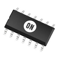
UC2843AD ON Semiconductor, UC2843AD Datasheet - Page 11

UC2843AD
Manufacturer Part Number
UC2843AD
Description
Other Power Management 52kHz 1A Current PWM
Manufacturer
ON Semiconductor
Type
High Performance Current Mode Controllersr
Datasheet
1.UC3843AN2.pdf
(18 pages)
Specifications of UC2843AD
Output Voltage Range
4.95 V to 5.05 V
Input Voltage Range
30 V
Operating Temperature Range
- 25 C to + 85 C
Mounting Style
SMD/SMT
Package / Case
SOIC-14
Lead Free Status / Rohs Status
Lead free / RoHS Compliant
Available stocks
Company
Part Number
Manufacturer
Quantity
Price
Company:
Part Number:
UC2843AD
Manufacturer:
MOTOROLA
Quantity:
8
Part Number:
UC2843AD
Manufacturer:
TI
Quantity:
20 000
Company:
Part Number:
UC2843AD1
Manufacturer:
MAXIM
Quantity:
4 415
Part Number:
UC2843AD8
Manufacturer:
TI/德州仪器
Quantity:
20 000
Company:
Part Number:
UC2843AD8/D8
Manufacturer:
UNITRODE
Quantity:
5 510
Company:
Part Number:
UC2843AD8TR
Manufacturer:
TI
Quantity:
12 500
Part Number:
UC2843AD8TR
Manufacturer:
TI/德州仪器
Quantity:
20 000
Part Number:
UC2843ADR2G
Manufacturer:
ON/安森美
Quantity:
20 000
Part Number:
UC2843ADTR
Manufacturer:
TI/德州仪器
Quantity:
20 000
wire−wrap or plug−in prototype boards. High Frequency
circuit layout techniques are imperative to prevent pulse
width jitter. This is usually caused by excessive noise
pick−up imposed on the Current Sense or Voltage Feedback
inputs. Noise immunity can be improved by lowering circuit
impedances at these points. The printed circuit layout should
contain a ground plane with low−current signal and
high−current switch and output grounds returning on
separate paths back to the input filter capacitor. Ceramic
bypass capacitors (0.1 mF) connected directly to V
and V
This provides a low impedance path for filtering the high
frequency noise. All high current loops should be kept as
short as possible using heavy copper runs to minimize
radiated EMI. The Error Amp compensation circuitry and
the converter output voltage divider should be located close
to the IC and as far as possible from the power switch and
other noise generating components.
oscillations when operating at a duty cycle greater than 50%
with continuous inductor current. This instability is
independent of the regulators closed−loop characteristics
and is caused by the simultaneous operating conditions of
fixed frequency and peak current detecting. Figure 20A
shows the phenomenon graphically. At t
conduction begins, causing the inductor current to rise at a
slope of m
divided by the inductance. At t
reaches the threshold established by the control voltage.
This causes the switch to turn off and the current to decay at
a slope of m
condition can be shown if a perturbation is added to the
control voltage, resulting in a small DI (dashed line). With
a fixed oscillator period, the current decay time is reduced,
and the minimum current at switch turn−on (t
by DI + DI m2/m1. The minimum current at the next cycle
Do not attempt to construct the converter on
Current mode converters can exhibit subharmonic
ref
may be required depending upon circuit layout.
1
. This slope is a function of the input voltage
2
until the next oscillator cycle. The unstable
1
, the Current Sense Input
UC3842A, UC3843A, UC2842A, UC2843A
2
DESIGN CONSIDERATIONS
) is increased
0
, switch
CC
http://onsemi.com
, V
C
,
11
(t
is multiplied by m
increasing and decreasing the inductor current at switch
turn−on. Several oscillator cycles may be required before
the inductor current reaches zero causing the process to
commence again. If m
will be unstable. Figure 20B shows that by adding an
artificial ramp that is synchronized with the PWM clock to
the control voltage, the DI perturbation will decrease to zero
on succeeding cycles. This compensation ramp (m
have a slope equal to or slightly greater than m
stability. With m
inductor current follows the control voltage yielding true
current mode operation. The compensating ramp can be
derived from the oscillator and added to either the Voltage
Feedback or Current Sense inputs (Figure 33).
3
) decreases to (DI +
Inductor
Current
DI
Control Voltage
Control Voltage
Figure 20. Continuous Current Waveforms
t
4
t
0
m1
Oscillator Period
2
DI + DI m
.m
2
/2 slope compensation, the average
DI
1
D
m1
2
on each succeeding cycle, alternately
I m
Oscillator Period
/m
m
m2
t
1
2
1
m3
2
1
/m
is greater than 1, the converter
1
(A)
(B)
) (m
t
5
t
m2
2
D I + DI
2
/m
1
). This perturbation
m
m
2
1
m
m
2
1
Inductor
Current
3
2
) must
t
/2 for
t
6
3


