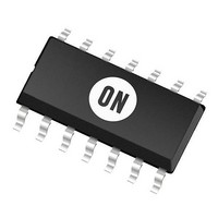
UC3844D ON Semiconductor, UC3844D Datasheet - Page 3

UC3844D
Manufacturer Part Number
UC3844D
Description
Other Power Management 52kHz 1A Current PWM
Manufacturer
ON Semiconductor
Type
High Performance Current Mode Controllersr
Datasheet
1.UC2845DR2.pdf
(16 pages)
Specifications of UC3844D
Output Voltage Range
4.9 V to 5.1 V
Input Voltage Range
30 V
Operating Temperature Range
0 C to + 70 C
Mounting Style
SMD/SMT
Package / Case
SOIC-14
Lead Free Status / Rohs Status
Lead free / RoHS Compliant
Available stocks
Company
Part Number
Manufacturer
Quantity
Price
Company:
Part Number:
UC3844D
Manufacturer:
MAXIM
Quantity:
113
Part Number:
UC3844D
Manufacturer:
UNITRO
Quantity:
20 000
Part Number:
UC3844D8
Manufacturer:
UC/TI
Quantity:
20 000
Company:
Part Number:
UC3844D8TR
Manufacturer:
TI
Quantity:
5 000
Part Number:
UC3844D8TR
Manufacturer:
TI/德州仪器
Quantity:
20 000
Company:
Part Number:
UC3844D8TRG4
Manufacturer:
TI
Quantity:
14 953
Part Number:
UC3844DB
Manufacturer:
UNITRODE
Quantity:
20 000
Part Number:
UC3844DG
Manufacturer:
ON/安森美
Quantity:
20 000
4. Adjust V
5. Low duty cycle pulse techniques are used during test to maintain junction temperature as close to ambient as possible.
6. This parameter is measured at the latch trip point with V
7. Comparator gain is defined as: A
ELECTRICAL CHARACTERISTICS
ERROR AMPLIFIER SECTION (continued)
CURRENT SENSE SECTION
OUTPUT SECTION
UNDERVOLTAGE LOCKOUT SECTION
PWM SECTION
TOTAL DEVICE
Unity Gain Bandwidth (T
Power Supply Rejection Ratio (V
Output Current
Output Voltage Swing
Current Sense Input Voltage Gain (Notes 6 & 7)
Maximum Current Sense Input Threshold (Note 6)
Power Supply Rejection Ratio
Input Bias Current
Propagation Delay (Current Sense Input to Output)
Output Voltage
Output Voltage with UVLO Activated
Output Voltage Rise Time (C
Output Voltage Fall Time (C
Startup Threshold
Minimum Operating Voltage After Turn−On
Duty Cycle
Power Supply Current (Note 4)
Power Supply Zener Voltage (I
T
Sink (V
Source (V
High State (R
Low State (R
V
Low State (I
High State (I
V
UCX844
UCX844
Maximum
Startup:
(V
(V
UCX845
UCX845
Minimum
low
CC
CC
CC
CC
= 0°C for UC3844, UC3845
= 12 V to 25 V (Note 6)
= 6.0 V, I
= 6.5 V for UCX845A,
14 V for UCX844) Operating
−25°C for UC2844, UC2845
O
CC
= 1.1 V, V
O
above the Startup threshold before setting to 15 V.
(I
(I
= 5.0 V, V
L
Sink
Sink
Sink
Sink
L
Sink
= 15 k to V
= 15 k to ground, V
Characteristics
= 20 mA)
= 200 mA)
= 20 mA)
= 200 mA)
= 1.0 mA
FB
FB
= 2.7 V)
J
= 25°C)
= 2.3 V)
ref
L
L
= 1.0 nF, T
, V
= 1.0 nF, T
CC
V
FB
CC
= 25 mA)
DV Output Compensation
= 2.7 V)
DV Current Sense Input
= 12 V to 25 V)
FB
= 2.3 V)
(V
J
J
= 25°C)
CC
= 25°C)
= 15 V, (Note 4), R
T
high
= +70°C for UC3844, UC3845
http://onsemi.com
+85°C for UC2844, UC2845
FB
= 0 V.
t
PLH(IN/OUT)
V
Symbol
V
OL(UVLO)
DC
I
PSRR
PSRR
DC
Source
CC(min)
T
I
V
V
V
V
BW
V
V
I
Sink
A
I
V
CC
= 10 k, C
OH
IB
OH
t
t
OL
OL
th
r
th
max
V
f
min
Z
3
T
= 3.3 nF, T
−0.5
2.85
Min
0.7
2.0
5.0
0.9
7.8
9.0
7.0
60
12
12
15
46
30
−
−
−
−
−
−
−
−
−
−
−
−
UC284X
−1.0
−2.0
13.5
13.4
Typ
150
A
1.0
6.2
0.8
3.0
1.0
0.1
1.6
0.1
8.4
7.6
0.5
70
12
70
50
50
16
10
48
12
36
−
= T
low
to T
Max
3.15
−10
300
150
150
1.1
1.1
0.4
2.2
1.1
9.0
8.2
1.0
17
11
50
17
−
−
−
−
−
−
−
−
0
−
high
(Note 5), unless otherwise noted.)
−0.5
2.85
14.5
Min
0.7
2.0
5.0
0.9
7.8
8.5
7.0
60
13
12
47
30
−
−
−
−
−
−
−
−
−
−
−
−
UC384X
−1.0
−2.0
13.5
13.4
Typ
150
1.0
6.2
0.8
3.0
1.0
0.1
1.6
0.1
8.4
7.6
0.5
70
12
70
50
50
16
10
48
12
36
−
Max
3.15
17.5
11.5
−10
300
150
150
1.1
1.1
0.4
2.2
1.1
9.0
8.2
1.0
50
17
−
−
−
−
−
−
−
−
0
−
MHz
Unit
V/V
mA
mA
dB
dB
mA
ns
ns
ns
%
V
V
V
V
V
V
V


