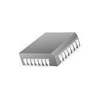
ML4812CQX Fairchild Semiconductor, ML4812CQX Datasheet - Page 2

ML4812CQX
Manufacturer Part Number
ML4812CQX
Description
Power Factor Correction ICs PFC Controller
Manufacturer
Fairchild Semiconductor
Datasheet
1.ML4812CQX.pdf
(17 pages)
Specifications of ML4812CQX
Switching Frequency
105 KHz
Maximum Operating Temperature
+ 70 C
Mounting Style
SMD/SMT
Package / Case
PLCC-20
Minimum Operating Temperature
0 C
Lead Free Status / Rohs Status
Lead free / RoHS Compliant
ML4812
Pin Configuration
Pin Description
2
Number
10
11
12
13
14
15
16
1
2
3
4
5
6
7
8
9
GM OUT
EA OUT
EA–
OVP
RAMP
COMP
R
CLOCK
SHDN
PWR
GND
OUT
V
V
GND
C
I
SINE
I
CC
REF
T
T
Name
SENSE
RAMP COMP
GM OUT
EA OUT
Input from the current sense transformer to the non-inverting input of the PWM
comparator.
Output of gain modulator. A resistor to ground on this pin converts the current to a
voltage. This pin is clamped to 5V and tied to the inverting input of the PWM comparator.
Output of error amplifier.
Inverting input to error amplifier.
Input to over voltage comparator.
Current gain modulator input.
Buffered output from the oscillator ramp (C
is internally subtracted from the product of I
Oscillator timing resistor pin. A 5V source sets a current in the external resistor which is
mirrored to charge C
Digital clock output.
A TTL compatible low level on this pin turns off the output.
Return for the high current totem pole output.
High current totem pole output.
Positive Supply for the IC.
Buffered output for the 5V voltage reference.
Analog signal ground.
Timing capacitor for the oscillator.
I SENSE
I SINE
OVP
16-Pin PDIP (P16)
EA–
R T
1
2
3
4
5
6
7
8
ML4812
Top View
16
15
14
13
12
11
10
9
C T
GND
V REF
V CC
OUT
PWR GND
SHDN
CLOCK
T
.
EA OUT
Function
I SINE
OVP
EA–
T
NC
SINE
). A resistor to ground sets the current which
20-Pin PLCC (Q20)
4
5
6
7
8
and I
3
9 10 11 12 13
ML4812
Top View
2
EA
1 20 19
in the gain modulator.
18
17
16
15
14
PRODUCT SPECIFICATION
V REF
V CC
NC
OUT
PWR GND
REV. 1.0.4 5/31/01


