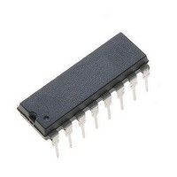
ML4802CP Fairchild Semiconductor, ML4802CP Datasheet - Page 9

ML4802CP
Manufacturer Part Number
ML4802CP
Description
Power Factor Correction ICs DIP-16
Manufacturer
Fairchild Semiconductor
Datasheet
1.ML4802CP.pdf
(15 pages)
Specifications of ML4802CP
Switching Frequency
212 KHz
Maximum Operating Temperature
+ 70 C
Mounting Style
Through Hole
Package / Case
PDIP-16
Minimum Operating Temperature
0 C
Lead Free Status / Rohs Status
Lead free / RoHS Compliant
Available stocks
Company
Part Number
Manufacturer
Quantity
Price
Part Number:
ML4802CP
Manufacturer:
ML
Quantity:
20 000
The output of the gain modulator is a current signal, in the
form of a full wave rectified sinusoid at twice the line
frequency. This current is applied to the virtual-ground
(negative) input of the current error amplifier. In this way
the gain modulator forms the reference for the current
error loop, and ultimately controls the instantaneous
current draw of the PFC from the power line. The general
form for the output of the gain modulator is:
More exactly, the output current of the gain modulator is
given by:
where K is in units of V
Note that the output current of the gain modulator is
limited to
Current Error Amplifier
The current error amplifier’s output controls the PFC duty
cycle to keep the current through the boost inductor a
linear function of the line voltage. At the inverting input
to the current error amplifier, the output current of the
gain modulator is summed with a current which results
from a negative voltage being impressed upon the ISENSE
pin (current into ISENSE @ VSENSE/1.8k
voltage on ISENSE represents the sum of all currents
flowing in the PFC circuit, and is typically derived from a
current sense resistor in series with the negative terminal
of the input bridge rectifier. As stated above, the ground.
Given this fact, and the arrangement of the duty cycle
modulator polarities internal to the PFC, an increase in
positive current from the gain modulator will cause the
output stage to increase its duty cycle until the voltage on
ISENSE is adequately negative to cancel this increased
current. Similarly, if the gain modulator’s output
decreases, the output duty cycle will decrease to achieve
a less negative voltage on the ISENSE pin.
There is a modest degree of gain contouring applied to the
transfer characteristic of the current error amplifier, to
increase its speed of response to current-loop
perturbations.
Cycle-By-Cycle Current Limiter
The ISENSE pin, as well as being a part of the current
feedback loop, is a direct input to the cycle-by-cycle
current limiter for the PFC section. Should the input
voltage at this pin ever be more negative than –1.5V, the
output of the PFC will be disabled until the protection
flip-flop is reset by the clock pulse at the start of the next
PFC power cycle.
REV. 1.0.1 12/12/2000
FUNCTIONAL DESCRIPTION (Continued)
IGAINMOD =
IGAINMOD = K
500 A.
IAC VEAO
™
VRMS
-1
0
™
VEAO - 0.625V
.
2
™
1
V
5
™
. The negative
IAC
Overvoltage Protection
The OVP comparator serves to protect the power circuit
from being subjected to excessive voltages if the load
should suddenly change. A resistor divider from the high
voltage DC output of the PFC is fed to VFB. When the
voltage on VFB exceeds 2.75V, the PFC output driver is
shut down. The PWM section will continue to operate. The
OVP comparator has 250mV of hysteresis, and the PFC
will not restart until the voltage at VFB drops below 2.5V.
The VFB should be set at a level where the active and
passive external power components and the ML4802 are
within their safe operating voltages, but not so low as to
interfere with the boost voltage regulation loop.
Error Amplifier Compensation
The PWM loading of the PFC can be modeled as a
negative resistor; an increase in input voltage to the PWM
causes a decrease in the input current. This response
dictates the proper compensation of the two
transconductance error amplifiers. Figure 4 shows the
types of compensation networks most commonly used for
the voltage and current error amplifiers, along with their
respective return points. The current loop compensation is
returned to VREF to produce a soft-start characteristic on
the PFC: as the reference voltage comes up from zero
volts, it creates a differentiated voltage on IEAO which
prevents the PFC from immediately demanding a full duty
cycle on its boost converter. This then works in
conjunction with the low output current of the VEA to
ensure low component stress at PFC startup.
OUTPUT
Figure 4. Compensation Network Connections for the
PFC
15
2
4
3
IAC
VFB
VRMS
ISENSE
2.5V
Voltage and Current Error Amplifiers
+
-
VEA
VEAO
MODULATOR
GAIN
16
1.6k
1.6k
+
–
IEA
IEAO
ML4802
VREF
1
+
-
9


