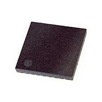
ispPAC-POWR6AT6-01N32I Lattice, ispPAC-POWR6AT6-01N32I Datasheet - Page 21

ispPAC-POWR6AT6-01N32I
Manufacturer Part Number
ispPAC-POWR6AT6-01N32I
Description
Supervisory Circuits Prec. Prog. Pwr Sppl y Seq. Mon. Trim I
Manufacturer
Lattice
Datasheet
1.ISPPAC-POWR6AT6-01NN32I.pdf
(35 pages)
Specifications of ispPAC-POWR6AT6-01N32I
Number Of Voltages Monitored
6
Output Type
Open Collector / Drain
Manual Reset
Not Resettable
Watchdog
No Watchdog
Power-up Reset Delay (typ)
500 ms
Supply Voltage (max)
3.96 V
Supply Voltage (min)
2.8 V
Supply Current (typ)
10 mA
Mounting Style
SMD/SMT
Package / Case
QFN-32
Lead Free Status / Rohs Status
Lead free / RoHS Compliant
Lattice Semiconductor
Writing a value to the ADC_MUX register to set the input attenuator and selector will automatically initiate a conver-
sion. When the conversion is in process, the DONE bit (ADC_VALUE_LOW.0) will be reset to 0. When the conver-
sion is complete, this bit will be set to 1. When the conversion is complete, the result may be read out of the ADC by
performing two I
mended that the I
command (Waiting for the DONE bit to be set to 1). An alternative would be to wait for a minimum specified time
(see Tconvert value in the specifications) and disregard checking the DONE bit.
Note that if the I
conversion is to wait the minimum specified time (Tconvert), as the operation of the DONE bit at clock rates lower
than that cannot be guaranteed. In other words, if the I
not assert even when a valid conversion result is available. Erroneous ADC readout results are also possible when-
ever the I
has elapsed. Under these conditions, it is still possible to obtain valid results for the second conversion by reading
out the ADC low and high byte results twice in succession (read ADC_VALUE_LOW, read ADC_VALUE_HIGH,
then repeating the low and high byte reads). Only the second ADC readout value is reliably valid, however.
To insure every ADC conversion result is valid, preferred operation is to clock I
DONE bit status or wait for the full T
request is placed before the current conversion is complete, the DONE bit will be set to 1 only after the second
request is complete.
The UES word may also be read through the I
Figure 3-17. I
The I
ing a write of any value to the I
section of this data sheet for further information.
2
C interface also provides the ability to initiate reset operations. The ispPAC-POWR6AT6 may be reset by issu-
2
C clock is less than 50kHz and a second ADC convert is commanded before a full T
2
C Register Mapping for UES Bits
2
C clock rate falls below 50kHz (see F
2
2
C read operations; one for ADC_VALUE_LOW, and one for ADC_VALUE_HIGH. It is recom-
C master load a second conversion command only after the completion of the current conversion
0x04 - UES_BYTE0 (Read Only)
0x05 - UES_BYTE1 (Read Only)
0x06 - UES_BYTE2 (Read Only)
0x07 - UES_BYTE3 (Read Only)
UES15
UES23
UES31
UES7
b7
b7
b7
b7
UES14
UES22
UES30
UES6
2
b6
b6
b6
b6
C RESET register (Figure 3-18). Refer to the RESET Command via JTAG or I
CONVERT
UES13
UES21
UES29
UES5
b5
b5
b5
b5
2
time period between subsequent ADC convert commands. If an I
C interface, with the register mapping shown in Figure 3-17.
UES12
UES20
UES28
UES4
b4
b4
b4
b4
I2C
3-21
2
C clock rate is less than 50kHz, the DONE bit may or may
note in specifications), the only way to insure a valid ADC
UES11
UES19
UES27
UES3
b3
b3
b3
b3
UES10
UES18
UES26
UES2
b2
b2
b2
b2
ispPAC-POWR6AT6 Data Sheet
UES17
UES25
UES1
UES9
2
b1
b1
b1
b1
C at more than 50kHz and verify
UES16
UES24
UES0
UES8
b0
b0
b0
b0
CONVERT
time period
2
2
C
C


