DS26LV31TM/NOPB National Semiconductor, DS26LV31TM/NOPB Datasheet - Page 2
DS26LV31TM/NOPB
Manufacturer Part Number
DS26LV31TM/NOPB
Description
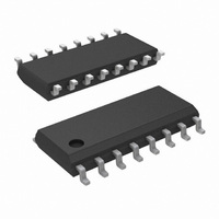
IC LINE DRIVER QUAD CMOS 16-SOIC
Manufacturer
National Semiconductor
Type
Driverr
Datasheet
1.DS26LV31TMXNOPB.pdf
(8 pages)
Specifications of DS26LV31TM/NOPB
Number Of Drivers/receivers
4/0
Protocol
RS422
Voltage - Supply
3 V ~ 3.6 V
Mounting Type
Surface Mount
Package / Case
16-SOIC (3.9mm Width)
Lead Free Status / RoHS Status
Lead free / RoHS Compliant
Other names
*DS26LV31TM
*DS26LV31TM/NOPB
DS26LV31TM
*DS26LV31TM/NOPB
DS26LV31TM
Available stocks
Company
Part Number
Manufacturer
Quantity
Price
Company:

Part Number:
DS26LV31TM/NOPB
Manufacturer:
Maxim
Quantity:
227


www.national.com
V
V
∆V
V
V
∆V
I
I
I
V
V
I
I
V
I
Symbol
OZ
SC
OFF
IH
IL
CC
OD1
OD2
OD3
OC
IH
IL
CL
Absolute Maximum Ratings
If Military/Aerospace specified devices are required,
please contact the National Semiconductor Sales Office/
Distributors for availability and specifications.
Electrical Characteristics
Over supply voltage and operating temperature ranges, unless otherwise specified
Supply Voltage (V
Enable Input Voltage (EN, EN*)
Driver Input Voltage (DI)
Clamp Diode Current
DC Output Current, per pin
Driver Output Voltage
Maximum Package Power Dissipaton
Derate M Package 9.8 mW/˚C above +25˚C
Derate W Package 7.5 mW/˚C above +25˚C
Storage Temperature Range
OD2
OC
(Power Off: DO+, DO−)
M Package
W Package
Output Differential Voltage
Output Differential Voltage
Change in Magnitude of
Output Differential Voltage
Output Differential Voltage
Common Mode Voltage
Change in Magnitude of
Common Mode Voltage
TRI-STATE Leakage
Current
Output Short Circuit Currrent
Output Leakage Current
High Level Input Voltage
Low Level Input Voltage
High Level Input Current
Low Level Input Current
Input Clamp Voltage
Power Supply Current
Parameter
CC
)
−0.5V to V
−0.5V to V
@
+25˚C
−65˚C to +150˚C
R
R
I
R
Figure 1 (Note 7)
R
V
Drivers Disabled
V
V
GND (Note 4)
V
V
−0.25V
V
V
I
No Load, V
= V
(Note 2) (Note 3)
O
IN
L
L
L
L
OUT
OUT
IN
CC
CC
IN
IN
≥ 20 mA
= −18 mA
=
= 100Ω (Figure 1)
= 3900Ω (V.11)
= 100Ω (Figure 1)
−0.5V to +7V
−0.5V to +7V
CC
= V
= V
= GND
= 0V, V
= 0V, V
(Note 1)
∞
= V
= 0V
or GND
CC
CC
1226 mW
±
1119 mW
CC
CC
(No Load)
±
150 mA
CC
+ 0.5V
+ 0.5V
20 mA
or
IN
OUT
OUT
or GND
Conditions
(all)
= 3V or 6V
=
T
+85˚C
T
+125˚C (Note 10)
T
+85˚C
T
+125˚C
T
+85˚C
T
+125˚C
2
A
A
A
A
A
A
= -40˚C to
= -55˚C to
= -40˚C to
= -55˚C to
= -40˚C to
= -55˚C to
Recommended Operating
Conditions
Supply Voltage (V
Operating Free Air Temperature Range (T
Input Rise and Fall Time
Lead Temperature Range
Soldering
(4 sec.)
ESD Ratings (HBM, 1.5 kΩ,
100 pF)
DS26LV31T
DS26LV31W
Driver Outputs
Other Pins
DO+,
DO−
EN*
V
EN,
Pin
DI,
CC
CC
)
−400
−400
GND
Min
−40
−10
-30
2.0
−55
2
Min
−40
3.0
+25
−0.08
Typ
±
+25
0.03
Typ
3.3
−70
3.3
2.6
3.2
1.5
0.5
7
6
+125
A
Max
+85
500
3.6
)
−150
−100
-160
-200
Max
−1.5
±
V
400
400
100
100
125
3.6
0.8
10
4
2
CC
20
˚C
≥2.5 kV
+260˚C
Units
≥7 kV
˚C
ns
V
Units
mV
mV
mA
mA
µA
µA
µA
µA
µA
µA
µA
µA
V
V
V
V
V
V
V
Related parts for DS26LV31TM/NOPB
Image
Part Number
Description
Manufacturer
Datasheet
Request
R

Part Number:
Description:
National Semiconductor [8-Bit D/A Converter]
Manufacturer:
National Semiconductor
Datasheet:
Part Number:
Description:
National Semiconductor [Media Coprocessor]
Manufacturer:
National Semiconductor
Datasheet:
Part Number:
Description:
Digitally Controlled Tone and Volume Circuit with Stereo Audio Power Amplifier, Microphone Preamp Stage and National 3D Sound
Manufacturer:
National Semiconductor
Datasheet:
Part Number:
Description:
Digitally Controlled Tone and Volume Circuit with Stereo Audio Power Amplifier, Microphone Preamp Stage and National 3D Sound
Manufacturer:
National Semiconductor
Datasheet:
Part Number:
Description:
AC97 Rev 2 Codec with Sample Rate Conversion and National 3D Sound
Manufacturer:
National Semiconductor
Part Number:
Description:
Manufacturer:
National Semiconductor
Datasheet:
Part Number:
Description:
Manufacturer:
National Semiconductor
Datasheet:
Part Number:
Description:
General Purpose, Low Voltage, Low Power, Rail-to-Rail Output Operational Amplifiers
Manufacturer:
National Semiconductor
Datasheet:
Part Number:
Description:
8-bit 20 MSPS flash A/D converter.
Manufacturer:
National Semiconductor
Datasheet:
Part Number:
Description:
Low Noise Quad Operational Amplifier
Manufacturer:
National Semiconductor
Datasheet:
Part Number:
Description:
Quad Differential Line Receivers
Manufacturer:
National Semiconductor
Datasheet:
Part Number:
Description:
Quad High Speed Trapezoidal? Bus Transceiver
Manufacturer:
National Semiconductor
Datasheet:
Part Number:
Description:
Dual Line Receiver
Manufacturer:
National Semiconductor
Datasheet:
Part Number:
Description:
TTL to 10k ECL Level Translator with Latch
Manufacturer:
National Semiconductor
Datasheet: