DS91M047TMAX/NOPB National Semiconductor, DS91M047TMAX/NOPB Datasheet - Page 3
DS91M047TMAX/NOPB
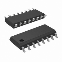
Manufacturer Part Number
DS91M047TMAX/NOPB
Description
IC LINE DRVR MLVDS QUAD 16-SOIC
Manufacturer
National Semiconductor
Type
Line Driver, Transmitterr
Datasheet
1.DS91M047TMANOPB.pdf
(12 pages)
Specifications of DS91M047TMAX/NOPB
Number Of Drivers/receivers
4/0
Protocol
LVDS
Voltage - Supply
3 V ~ 3.6 V
Mounting Type
Surface Mount
Package / Case
16-SOIC (3.9mm Width)
Lead Free Status / RoHS Status
Lead free / RoHS Compliant
Other names
DS91M047TMAX
Available stocks
Company
Part Number
Manufacturer
Quantity
Price
Company:

Part Number:
DS91M047TMAX/NOPB
Manufacturer:
NS/TI
Quantity:
130


LVCMOS DC Specifications
V
V
I
I
V
M-LVDS DC Specifications
|V
ΔV
V
|ΔV
V
V
V
V
I
I
I
I
IH
IL
OS
A
B
AB
IH
IL
CL
OS(SS)
A(OC)
B(OC)
P(H)
P(L)
Symbol
AB
Absolute Maximum Ratings
If Military/Aerospace specified devices are required,
please contact the National Semiconductor Sales Office/
Distributors for availability and specifications.
DC Electrical Characteristics
Over supply voltage and operating temperature ranges, unless otherwise specified.
Power Supply Voltage
LVCMOS Input Voltage
M-LVDS Output Voltage
M-LVDS Output Short Circuit
Current Duration
Junction Temperature
Storage Temperature Range
Lead Temperature Range
Maximum Package Power Dissipation @ +25°C
Package Thermal Resistance (4-Layer, 2 oz. Cu, JEDEC)
θ
θ
AB
OS(SS)
|
Soldering (4 sec.)
MA Package
Derate MA Package
JA
JC
|
High-Level Input Voltage
Low-Level Input Voltage
High-Level Input Current
Low-Level Input Current
Input Clamp Voltage
Differential Output Voltage Magnitude
Change in Differential Output Voltage Magnitude
Between Logic States
Steady-State Common-Mode Output Voltage
Change in Steady-State Common-Mode Output
Voltage Between Logic States
Maximum Steady-State Open-Circuit Output Voltage
Maximum Steady-State Open-Circuit Output Voltage
Voltage Overshoot, Low-to-High Level Output
(Note
Voltage Overshoot, High-to-Low Level Output
(Note
Output Short-Circuit Current
Driver High-Impedance Output Current
Driver High-Impedance Output Current
Driver High-Impedance Output Differential Curent
(I
A
− I
B
10)
10)
)
Parameter
19.2 mW/°C above +25°C
−0.3V to (V
(Note
−65°C to +150°C
−1.9V to +5.5V
8)
−0.3V to +4V
(Note
Continuous
DD
+52°C/W
+19°C/W
(Note
+140°C
+260°C
+ 0.3V)
2.21W
4)
5,
Note
3
6,
V
V
I
R
Figures 1, 3
Figures 1, 2
R
Figure 4
R
C
Figure 5
V
V
V
V
V
V
V
IN
IH
IL
A
A
A
A
A
A
A
L
L
L
D
Note
Note 1: Human Body Model, applicable std. JESD22-A114C
Note 2: Machine Model, applicable std. JESD22-A115-A
Note 3: Field Induced Charge Device Model, applicable std.
JESD22-C101-C
Recommended
OperatingConditions
= -18 mA
= 50Ω, C
= 50Ω
= 50Ω, C
= 3.8V, V
= 0V or 2.4V, V
= −1.4V, V
= 3.8V, V
= 0V or 2.4V, V
= −1.4V, V
= V
ESD Susceptibility
Supply Voltage (VDD)
Voltage at Any Bus Terminal
(Separate or Common-Mode)
High Level Input Voltage (V
Low Level Input Voltage (V
Operating Free Air
= 0.5 pF, Figures 6, 7
= 0V
= 3.6V
HBM
MM
CDM
Temperature (T
B
7,
, −1.4V
Conditions
Note
L
L
B
B
= 5 pF
= 5 pF
B
B
= 1.2V
= 1.2V
9)
= 1.2V
= 1.2V
≤
V
B
B
≤
= 1.2V
= 1.2V
A
3.8V
)
−0.2V
IL
IH
GND
)
0.30
Min
-1.5
−50
−20
−32
−20
−32
480
-15
-15
-43
)
2.0
−4
0
0
0
0
0
SS
+3.0 +3.3 +3.6
−1.4
Min
−40
2.0
0
Typ
1.6
±1
±1
Typ Max Units
+25
1.2V
+3.8
V
+85
Max
2.10
0.8
V
650
0.8
2.4
2.4
www.national.com
15
15
50
50
43
32
20
32
20
DD
0
0
4
DD
SS
≥
≥
1250V
≥
250V
8 kV
°C
V
V
V
V
Units
mV
mV
mV
mA
μA
μA
μA
μA
μA
μA
μA
μA
μA
V
V
V
V
V
V
V
V
Related parts for DS91M047TMAX/NOPB
Image
Part Number
Description
Manufacturer
Datasheet
Request
R

Part Number:
Description:
National Semiconductor [8-Bit D/A Converter]
Manufacturer:
National Semiconductor
Datasheet:
Part Number:
Description:
National Semiconductor [Media Coprocessor]
Manufacturer:
National Semiconductor
Datasheet:
Part Number:
Description:
Digitally Controlled Tone and Volume Circuit with Stereo Audio Power Amplifier, Microphone Preamp Stage and National 3D Sound
Manufacturer:
National Semiconductor
Datasheet:
Part Number:
Description:
Digitally Controlled Tone and Volume Circuit with Stereo Audio Power Amplifier, Microphone Preamp Stage and National 3D Sound
Manufacturer:
National Semiconductor
Datasheet:
Part Number:
Description:
AC97 Rev 2 Codec with Sample Rate Conversion and National 3D Sound
Manufacturer:
National Semiconductor
Part Number:
Description:
Manufacturer:
National Semiconductor
Datasheet:
Part Number:
Description:
Manufacturer:
National Semiconductor
Datasheet:
Part Number:
Description:
General Purpose, Low Voltage, Low Power, Rail-to-Rail Output Operational Amplifiers
Manufacturer:
National Semiconductor
Datasheet:
Part Number:
Description:
8-bit 20 MSPS flash A/D converter.
Manufacturer:
National Semiconductor
Datasheet:
Part Number:
Description:
Low Noise Quad Operational Amplifier
Manufacturer:
National Semiconductor
Datasheet:
Part Number:
Description:
Quad Differential Line Receivers
Manufacturer:
National Semiconductor
Datasheet:
Part Number:
Description:
Quad High Speed Trapezoidal? Bus Transceiver
Manufacturer:
National Semiconductor
Datasheet:
Part Number:
Description:
Dual Line Receiver
Manufacturer:
National Semiconductor
Datasheet:
Part Number:
Description:
TTL to 10k ECL Level Translator with Latch
Manufacturer:
National Semiconductor
Datasheet: