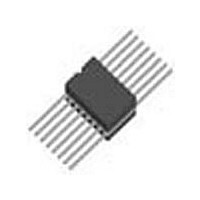
DS90C032W-QML National Semiconductor, DS90C032W-QML Datasheet - Page 9

DS90C032W-QML
Manufacturer Part Number
DS90C032W-QML
Description
Manufacturer
National Semiconductor
Datasheet
1.DS90C032W-QML.pdf
(14 pages)
Specifications of DS90C032W-QML
Number Of Elements
4
Number Of Receivers
4
Number Of Drivers
4
Operating Supply Voltage (typ)
5V
Differential Input High Threshold Voltage
100mV
Diff. Input Low Threshold Volt
-100mV
Propagation Delay Time
8ns
Power Dissipation
1.4W
Operating Temp Range
-55C to 125C
Operating Temperature Classification
Military
Mounting
Surface Mount
Pin Count
16
Lead Free Status / Rohs Status
Not Compliant
Typical Application
Applications Information
LVDS drivers and receivers are intended to be primarily used
in an uncomplicated point-to-point configuration as is shown
in Figure 5. This configuration provides a clean signaling en-
vironment for the quick edge rates of the drivers. The receiver
is connected to the driver through a balanced media which
may be a standard twisted pair cable, a parallel pair cable, or
simply PCB traces. Typically the characteristic impedance of
the media is in the range of 100Ω. A termination resistor of
100Ω should be selected to match the media, and is located
as close to the receiver input pins as possible. The termination
resistor converts the current sourced by the driver into a volt-
age that is detected by the receiver. Other configurations are
possible such as a multi-receiver configuration, but the effects
of a mid-stream connector(s), cable stub(s), and other
impedance discontinuities as well as ground shifting, noise
Pin Descriptions
Pin No. (SOIC)
2, 6, 10, 14
3, 5, 11, 13
1, 7, 9, 15
12
16
4
8
Power Supply Voltage
Transition Time vs
Name
Gnd
EN*
V
R
R
EN
R
CC
I+
I−
O
FIGURE 5. Point-to-Point Application
Description
Non-inverting receiver input pin
Inverting receiver input pin
Receiver output pin
Active high enable pin, OR-ed with EN*
Active low enable pin, OR-ed with EN
Power supply pin, +5V ± 10%
Ground pin
20163718
9
margin limits, and total termination loading must be taken into
account.
The DS90C032 differential line receiver is capable of detect-
ing signals as low as 100 mV, over a ±1V common-mode
range centered around +1.2V. This is related to the driver off-
set voltage which is typically +1.2V. The driven signal is
centered around this voltage and may shift ±1V around this
center point. The ±1V shifting may be the result of a ground
potential difference between the driver's ground reference
and the receiver's ground reference, the common-mode ef-
fects of coupled noise, or a combination of the two. Both
receiver input pins should honor their specified operating in-
put voltage range of 0V to +2.4V (measured from each pin to
ground), exceeding these limits may turn on the ESD protec-
tion circuitry which will clamp the bus voltages.
Ambient Temperature
Transition Time vs
20163707
20163719
www.national.com


