DLP-2232H DLP Design Inc, DLP-2232H Datasheet - Page 11
DLP-2232H
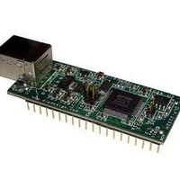
Manufacturer Part Number
DLP-2232H
Description
Interface Modules & Development Tools Dual Ch USB Adapter w/ FTDI FT2232H
Manufacturer
DLP Design Inc
Series
-r
Datasheet
1.DLP-2232H.pdf
(17 pages)
Specifications of DLP-2232H
Interface Type
USB, I2C, JTAG, SPI, UART
Description/function
High Speed USB Adapter
Dimensions
57.8 mm x 23.5 mm
Maximum Operating Temperature
+ 85 C
Minimum Operating Temperature
- 40 C
Number Of Channels
2
Product
Interface Modules
Supply Current
75 mA
Supply Voltage (max)
5 V
Supply Voltage (min)
4 V
Main Purpose
Interface, USB 2.0 to UART (RS232) Bridge
Embedded
No
Utilized Ic / Part
FT2232H
Primary Attributes
Full Speed USB to High-Speed UART
Secondary Attributes
Royalty-Free Drivers, 2K EEPROM
Lead Free Status / Rohs Status
Lead free / RoHS Compliant


Rev. 1.1 (May 2011)
22
23
26
27
28
29
30
31
32
33
34
35
36
37
38
39
40
GROUND
GROUND
PORT A OE# - Output enable: when low drive data onto D0-7. This should be driven low
at least 1 clock period before driving RD# low to allow for data buffer turn around.
PORT A CLKOUT – 60 MHz Clock driven from the FTDI chip. All signals should be
synchronized to this clock.
SIWUA –The Port A Send Immediate / WakeUp signal combines two functions on a
single pin. If USB is in suspend mode (PWREN# = 1) and remote wakeup is enabled in
the EEPROM, strobing this pin low will cause the device to request a resume on the USB
Bus. Normally, this can be used to wake up the Host PC. During normal operation
(PWREN# = 0), if this pin is strobed low any data in the device TX buffer will be sent out
over USB on the next Bulk-IN request from the drivers regardless of the pending packet
size. This can be used to optimize USB transfer speed for some applications. Tie this pin
to VCCIO if not used.
PORT A WR# - When taken from a high to a low state, WR reads the 8 data lines and
writes the byte into the FIFO’s transmit buffer. Data written to the transmit buffer is sent
to the host PC within the TX buffer timeout value (default 16mS) and placed in the buffer
that was created when the USB port was opened.
PORT A RD# - When pulled low, RD# takes the 8 data lines from a high-impedance
state to the current byte in the FIFO’s buffer. Taking RD# high returns the data pins to a
high- impedance state and prepares the next byte (if available) in the FIFO to be read.
PORT A TXE# - Transmit Buffer Empty: When high, do not write data into the FIFO.
When low, data can be written into the FIFO by strobing WR high, then low. During reset
this signal pin is tri-state. Data is latched into the FIFO on the falling edge of the WR pin.
PORT A RXF# - Receive Buffer Full : When low, at least 1 byte is present in the FIFO’s
receive buffer and is ready to be read with RD#. RXF# goes high when the receive buffer is
empty. During reset this signal pin is tri-state. If the Remote Wakeup option is enabled in the
internal EEPROM, during USB Suspend Mode (PWREN#=1) RXF# becomes an input. This can
be used to wake up the USB host from Suspend Mode by strobing this pin low for a minimum of
20ms which will cause the device to request a resume on the USB bus.
PORT A DB7 – Port A FIFO Data Bus Bit 7
PORT A DB6 – Port A FIFO Data Bus Bit 6
PORT A DB5 – Port A FIFO Data Bus Bit 5
PORT A DB4 – Port A FIFO Data Bus Bit 4
PORT A DB3 – Port A FIFO Data Bus Bit 3
PORT A DB2 – Port A FIFO Data Bus Bit 2
PORT A DB1 – Port A FIFO Data Bus Bit 1
PORT A DB0 – Port A FIFO Data Bus Bit 0
11
© DLP Design, Inc.
Related parts for DLP-2232H
Image
Part Number
Description
Manufacturer
Datasheet
Request
R

Part Number:
Description:
Zigbee / 802.15.4 Modules & Development Tools USE 626-DLP-RF2-Z
Manufacturer:
DLP Design Inc
Datasheet:
Part Number:
Description:
Zigbee / 802.15.4 Modules & Development Tools TTL SERIAL INTERFACE MODULE
Manufacturer:
DLP Design Inc
Datasheet:

Part Number:
Description:
MODULE USB-TO-TTL SRL UART CONV
Manufacturer:
DLP Design Inc
Datasheet:

Part Number:
Description:
Interface Modules & Development Tools FLASH2 TARGET BOARD 18F2321 w/IDE 2k Ltd
Manufacturer:
DLP Design Inc

Part Number:
Description:
Interface Modules & Development Tools FLASH2 TARGET BOARD 16F917 w/IDE 2k Ltd
Manufacturer:
DLP Design Inc

Part Number:
Description:
Interface Modules & Development Tools FLASH2 TARGET BOARD 18F4420 w/IDE 2k Ltd
Manufacturer:
DLP Design Inc
Part Number:
Description:
Zigbee / 802.15.4 Modules & Development Tools TTL SERIAL INTERFACE MODULE
Manufacturer:
DLP Design Inc
Datasheet:

Part Number:
Description:
Interface Modules & Development Tools USB FPGA Module w/ Xilinx XC3S400A
Manufacturer:
DLP Design Inc
Datasheet:

Part Number:
Description:
MODULE DATA-ACQUISITION 8-CH
Manufacturer:
DLP Design Inc
Datasheet:

Part Number:
Description:
MODULE DATA-ACQUISITION 20-CH
Manufacturer:
DLP Design Inc
Datasheet:

Part Number:
Description:
MODULE USB-MCU FT245RL W/16F877A
Manufacturer:
DLP Design Inc
Datasheet:

Part Number:
Description:
MODULE USB-TO-FPGA TRAINING TOOL
Manufacturer:
DLP Design Inc
Datasheet:

Part Number:
Description:
MODULE USB-MCU FT232R W/18F2410
Manufacturer:
DLP Design Inc
Datasheet:

Part Number:
Description:
MODULE USB-MCU FT245RL W/SX48
Manufacturer:
DLP Design Inc
Datasheet:

Part Number:
Description:
MODULE USB-MCU FT2232D W/16F877A
Manufacturer:
DLP Design Inc
Datasheet: