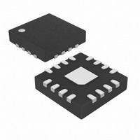
MAX3450EETE+ Maxim Integrated Products, MAX3450EETE+ Datasheet - Page 10

MAX3450EETE+
Manufacturer Part Number
MAX3450EETE+
Description
TXRX USB +/-15KV ESD PROT 16TQFN
Manufacturer
Maxim Integrated Products
Type
Transceiverr
Datasheet
1.MAX3451EEUD.pdf
(14 pages)
Specifications of MAX3450EETE+
Number Of Drivers/receivers
1/1
Protocol
USB 2.0
Voltage - Supply
3 V ~ 3.6 V
Mounting Type
Surface Mount
Package / Case
16-TQFN Exposed Pad
Lead Free Status / RoHS Status
Lead free / RoHS Compliant
±15kV ESD-Protected USB Transceivers
The push-pull bus detect (BD) output monitors V
and asserts high if V
asserts low if V
MAX3452E enters sharing mode (Table 2).
An internal linear regulator generates the V
(+3.3V typ). V
Power-Supply Configurations section). V
internal portions of the USB circuitry and provides the
pullup voltage for an external USB pullup resistor
MAX3450E/MAX3452E. Bypass V
ceramic capacitor as close to the device as possible.
Do not use V
D+ and D- serve as bidirectional bus connections and
are ESD protected to ±15kV (Human Body Model). For
OE = low, D+ and D- serve as transmitter outputs. For
OE = high, D+ and D- serve as receiver inputs.
For most applications, V
minal on the USB connector. V
an external supply as low as +3.1V (MAX3450E and
MAX3451E). See the Power-Supply Configurations sec-
tion. Drive V
V
to the device as possible.
Proper USB operation requires two external resistors,
each 24.3Ω ±1%, 1/8W (or greater). Install one resistor
in series between D+ of the MAX3450E/MAX3451E/
MAX3452E and D+ on the USB connector. Install the
other resistor in series between D- of the MAX3450E/
MAX3451E/MAX3452E and D- on the USB connector
(see the Typical Operating Circuit ).
Table 4b. Receive Truth Table
( OE = 1 and SUS = 1)
10
BUS
D+
0
0
1
1
INPUTS
______________________________________________________________________________________
to GND with a 0.1µF ceramic capacitor as close
D-
0
1
0
1
TRM
BUS
TRM
VP
to provide power to external circuitry.
low to enable sharing mode. Bypass
0
0
1
1
BUS
derives power from V
OUTPUTS
BUS
is less than +3.6V and the
VM
BUS
0
1
0
1
is greater than +4.0V. BD
External Components
connects to the V
RCV
BUS
0
0
0
0
TRM
can also connect to
External Resistors
to GND with a 1µF
BD (MAX3452E)
OUTPUT STATE
TRM
Undefined
BUS
Logic 0
Logic 1
TRM
SE0
powers the
D+ and D-
(see the
BUS
voltage
V
V
TRM
BUS
BUS
ter-
The MAX3450E/MAX3452E requires an external 1.5kΩ
pullup resistor between V
bus speed.
The MAX3450E/MAX3451E/MAX3452E require three
external capacitors for proper operation. Bypass V
GND with a 0.1µF ceramic capacitor. Bypass V
GND with a 0.1µF ceramic capacitor. Bypass V
GND with a 1µF (min) ceramic capacitor. Install all capac-
itors as close to the device as possible.
The MAX3450E/MAX3451E/MAX3452E transmit data to
the USB differentially on D+ and D-. VP and VM serve as
differential input signals to the driver (Tables 3a and 3b).
To receive data from the USB, drive OE high and SUS
low. Differential data received by D+ and D- appears
as a differential logic signal at RCV. Single-ended
receivers on D+ and D- drive VP and VM, respectively
(Tables 4a and 4b).
Figure 2. Timing of VP and VM to D+ and D-
VM
VP
D+
D-
t
PLH_DRV
Transmitting Data to the USB
V
Receiving Data from the USB
CRS_F
TRM
, V
CRS_L
and D+ or D- to set the
VP AND VM RISE/FALL TIMES < 4ns
t
External Capacitors
PHL_DRV
Data Transfer
TRM
BUS
L
to
to
to


