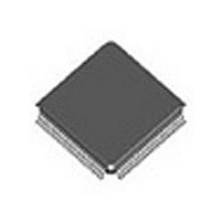
GS816018BT-150 GSI TECHNOLOGY, GS816018BT-150 Datasheet - Page 19

GS816018BT-150
Manufacturer Part Number
GS816018BT-150
Description
Manufacturer
GSI TECHNOLOGY
Datasheet
1.GS816018BT-150.pdf
(23 pages)
Specifications of GS816018BT-150
Density
18Mb
Access Time (max)
7.5ns
Sync/async
Synchronous
Architecture
SDR
Clock Freq (max)
133.3MHz
Operating Supply Voltage (typ)
2.5/3.3V
Address Bus
20b
Package Type
TQFP
Operating Temp Range
0C to 70C
Number Of Ports
2
Supply Current
175mA
Operating Supply Voltage (min)
2.3/3V
Operating Supply Voltage (max)
2.7/3.6V
Operating Temperature Classification
Commercial
Mounting
Surface Mount
Pin Count
100
Word Size
18b
Number Of Words
1M
Lead Free Status / Rohs Status
Not Compliant
Available stocks
Company
Part Number
Manufacturer
Quantity
Price
Company:
Part Number:
GS816018BT-150
Manufacturer:
PULSE
Quantity:
50 000
Sleep Mode
During normal operation, ZZ must be pulled low, either by the user or by its internal pull down resistor. When ZZ is pulled high,
the SRAM will enter a Power Sleep mode after 2 cycles. At this time, internal state of the SRAM is preserved. When ZZ returns to
low, the SRAM operates normally after ZZ recovery time.
Sleep mode is a low current, power-down mode in which the device is deselected and current is reduced to I
Sleep mode is dictated by the length of time the ZZ is in a High state. After entering Sleep mode, all inputs except ZZ become
disabled and all outputs go to High-Z The ZZ pin is an asynchronous, active high input that causes the device to enter Sleep mode.
When the ZZ pin is driven high, I
operations or operations in progress may not be properly completed if ZZ is asserted. Therefore, Sleep mode must not be initiated
until valid pending operations are completed. Similarly, when exiting Sleep mode during tZZR, only a Deselect or Read commands
may be applied while the SRAM is recovering from Sleep mode.
Application Tips
Single and Dual Cycle Deselect
SCD devices (like this one) force the use of “dummy read cycles” (read cycles that are launched normally but that are ended with
the output drivers inactive) in a fully synchronous environment. Dummy read cycles waste performance but their use usually
assures there will be no bus contention in transitions from reads to writes or between banks of RAMs. DCD SRAMs do not waste
bandwidth on dummy cycles and are logically simpler to manage in a multiple bank application (wait states need not be inserted at
bank address boundary crossings) but greater care must be exercised to avoid excessive bus contention.
Rev: 1.05 9/2008
Specifications cited are subject to change without notice. For latest documentation see http://www.gsitechnology.com.
ADSC
ADSP
CK
ZZ
Setup
Hold
SB
2 is guaranteed after the time tZZI is met. Because ZZ is an asynchronous input, pending
tKC
tKC
tKH
tKH
tKL
tKL
Sleep Mode Timing
19/23
tZZS
tZZH
GS816018/32/36BT-250/200/150
tZZR
SB
© 2004, GSI Technology
2. The duration of


