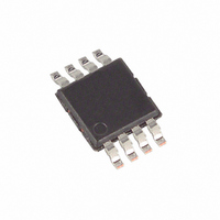
MAX1483CUA+T Maxim Integrated Products, MAX1483CUA+T Datasheet - Page 2

MAX1483CUA+T
Manufacturer Part Number
MAX1483CUA+T
Description
IC TXRX RS485/RS422 LP 8-UMAX
Manufacturer
Maxim Integrated Products
Type
Transceiverr
Datasheet
1.MAX1483CSA.pdf
(14 pages)
Specifications of MAX1483CUA+T
Number Of Drivers/receivers
1/1
Protocol
RS422, RS485
Voltage - Supply
4.75 V ~ 5.25 V
Mounting Type
Surface Mount
Package / Case
8-MSOP, Micro8™, 8-uMAX, 8-uSOP,
Lead Free Status / RoHS Status
Lead free / RoHS Compliant
ABSOLUTE MAXIMUM RATINGS
Supply Voltage (V
Control Input Voltages (RE, DE) .................-0.5V to (V
Driver Input Voltage (DI).............................-0.5V to (V
Driver Output Voltages ..........................................-7.5V to 12.5V
Receiver Input Voltages (A, B) ..............................-7.5V to 12.5V
Receiver Output Voltage (RO)....................-0.5V to (V
Continuous Power Dissipation (T
20µA,
RS-485 Transceivers
DC ELECTRICAL CHARACTERISTICS
(V
Stresses beyond those listed under “Absolute Maximum Ratings” may cause permanent damage to the device. These are stress ratings only, and functional
operation of the device at these or any other conditions beyond those indicated in the operational sections of the specifications is not implied. Exposure to
absolute maximum rating conditions for extended periods may affect device reliability.
Note 1: All currents into device pins are positive; all currents out of device pins are negative. All voltages are referenced to device
2
Differential Driver Output (no load)
Differential Driver Output
(with load)
8-Pin Plastic DIP (derate 9.09mW/°C above +70°C) .....727mW
14-Pin Plastic DIP (derate 10.00mW/°C above +70°C) .800mW
Change in Magnitude of Driver
Differential Output Voltage for
Complementary Output States
Driver Common-Mode Output
Voltage
Change in Magnitude of Driver
Common-Mode Output Voltage
for Complementary Output States
Three-State (high impedance)
Output Current at Driver
Logic Input High Voltage
Logic Input Low Voltage
Logic Input Current
Input Current
(A, B)
Receiver Differential Threshold
Voltage
Receiver Input Hysteresis
Receiver Output High Voltage
Receiver Output Low Voltage
Three-State (high impedance)
Output Current at Receiver
Receiver Input Resistance
CC
_______________________________________________________________________________________
= 5V ±5%, T
ground unless otherwise specified.
PARAMETER
1
CC
A
= T
) ...............................................................7V
⁄
8
MIN
-Unit-Load, Slew-Rate-Limited
to T
MAX
A
= +70°C)
, unless otherwise noted. Typical values are at T
SYMBOL
V
V
I
I
V
V
V
V
OZD
I
I
V
OZR
R
V
V
V
OD2
V
IN1
IN2
OD1
OC
OH
OL
TH
IH
IL
IN
OD
OD
TH
R = 50 (RS-422), Figure 1
R = 27 (RS-485), Figure 1
R = 27 or 50 , Figure 1
R = 27 or 50 , Figure 1
R = 27 or 50 , Figure 1
MAX1482 only,
-7V < V
DE, DI,
DE, DI,
DE, DI,
MAX1482,
DE = 0V, V
MAX1483,
DE = 0V, V
-7V
V
I
I
0.4V
-7V
O
O
CM
= 4mA, V
= -4mA, V
= 0V
CC
CC
CC
V
V
V
CM
CM
Y and
–
R
–
R
–
R
—
—
—
O
+ 0.5V)
+ 0.5V)
+ 0.5V)
E
E
E
–
–
–
CC
CC
ID
2.4V
12V
12V
ID
V
Z
= 0V or 5.25V
= 0V or 5.25V
= -200mV
= 200mV
CONDITIONS
< 12V
Operating Temperature Ranges
Storage Temperature Range .............................-65°C to +160°C
Lead Temperature (soldering, 10sec) .............................+300°C
8-Pin SO (derate 5.88mW/°C above +70°C)..................471mW
14-Pin SO (derate 8.33mW/°C above +70°C)................667mW
8-Pin µMAX (derate 4.10mW/°C above +70°C) .............330mW
MAX148_C_ _ .......................................................0°C to +70°C
MAX148_E_ _.....................................................-40°C to +85°C
V
V
V
V
IN
IN
IN
IN
= 12V
= -7V
= 12V
= -7V
A
= +25°C.) (Note 1)
MIN
-0.2
1.5
2.0
3.5
96
2
TYP
75
MAX
-100
-150
±50
150
200
0.2
0.2
0.8
0.2
0.4
±2
±1
5
5
5
3
UNITS
mV
µA
µA
µA
µA
k
V
V
V
V
V
V
V
V
V
V


