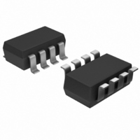
MAX9171EKA+T Maxim Integrated Products, MAX9171EKA+T Datasheet - Page 6

MAX9171EKA+T
Manufacturer Part Number
MAX9171EKA+T
Description
IC RECEIVER LVDS LINE SOT23-8
Manufacturer
Maxim Integrated Products
Type
Receiverr
Datasheet
1.MAX9171EKAT.pdf
(12 pages)
Specifications of MAX9171EKA+T
Number Of Drivers/receivers
0/1
Protocol
LVDS
Voltage - Supply
3 V ~ 3.6 V
Mounting Type
Surface Mount
Package / Case
SOT-23-8
Lead Free Status / RoHS Status
Lead free / RoHS Compliant
The MAX9171/MAX9172 feature LVDS inputs for inter-
facing high-speed digital circuitry. The LVDS interface
standard is a signaling method intended for point-to-
point communication over controlled-impedance
media, as defined by the ANSI TIA/EIA-644 standards.
The technology uses low-voltage signals to achieve fast
transition times and minimize power dissipation and
noise immunity. The MAX9171/MAX9172 convert LVDS
Single/Dual LVDS Line Receivers with
“In-Path” Fail-Safe
Table 1. Input-Output Function Table
6
Undriven parallel termination
SOT23
SOT23
4, 5, 6
_______________________________________________________________________________________
—
—
1
2
3
7
8
1
2
3
4
5
6
7
8
Undriven short
(IN_+) - (IN_-)
≤ -100mV
PIN
PIN
INPUTS
≥ 0mV
Open
( TD FN onl y)
( TD FN onl y)
SO/TDFN
SO/TDFN
3, 4, 6
8
5
7
2
1
8
5
7
6
4
3
2
1
Detailed Description
NAME
NAME
OUT1
OUT2
GND
OUT
N.C.
GND
IN2+
IN1+
V
IN+
V
IN2-
IN1-
IN-
EP
EP
CC
CC
Positive Power-Supply Input. Bypass with a 0.1µF and a 0.001µF capacitor to GND with the
smallest capacitor closest to the pin.
Ground
Receiver Output
No Connection. Not internally connected.
Noninverting Differential Receiver Input
Inverting Differential Receiver Input
Exposed Paddle. Solder to PCB ground.
Positive Power-Supply Input. Bypass with a 0.1µF and a 0.001µF capacitor to GND with the
smallest capacitor closest to the pin.
Ground
Receiver Output 1
Receiver Output 2
Inverting Differential Receiver Input 2
Noninverting Differential Receiver Input 2
Noninverting Differential Receiver Input 1
Inverting Differential Receiver Input 1
Exposed Paddle. Solder to PCB ground.
OUTPUT
OUT_
LVDS Inputs
High
High
High
High
Low
signals to LVCMOS/LVTTL signals at rates in excess of
500Mbps. These devices are capable of detecting dif-
ferential signals as low as 100mV and as high as 1.2V
within a 0 to V
input-output function table.
The MAX9171/MAX9172 fail-safe drives the receiver
output high when the differential input is:
• Open
• Undriven and shorted
• Undriven and terminated
Without fail-safe, differential noise at the input may
switch the receiver and appear as data to the receiving
system. An open input occurs when a cable and termi-
nation are disconnected. An undriven, terminated input
occurs when a cable is disconnected with the termina-
tion still connected across the receiver inputs or when
the driver of a receiver is in high impedance. An undriv-
en, shorted input can occur due to a shorted cable.
FUNCTION
FUNCTION
MAX9171 Pin Description
MAX9172 Pin Description
CC
input voltage range. Table 1 is the
Fail-Safe


