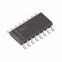
MAX4444ESE+T Maxim Integrated Products, MAX4444ESE+T Datasheet - Page 2

MAX4444ESE+T
Manufacturer Part Number
MAX4444ESE+T
Description
IC LINE RCVR DIFF-SGL 16-SOIC
Manufacturer
Maxim Integrated Products
Type
Receiverr
Datasheet
1.MAX4445ESE.pdf
(8 pages)
Specifications of MAX4444ESE+T
Number Of Drivers/receivers
0/1
Voltage - Supply
4.5 V ~ 5.5 V
Mounting Type
Surface Mount
Package / Case
16-SOIC (3.9mm Width)
Lead Free Status / RoHS Status
Lead free / RoHS Compliant
Protocol
-
ABSOLUTE MAXIMUM RATINGS
V
Voltage on IN+, IN-, EN, OUT+,
Current Into IN+, IN-, RG, EN .............................................20mA
Output Short-Circuit Duration ...........................Indefinite to GND
Ultra-High-Speed, Low-Distortion, Differential-
to-Single-Ended Line Receivers with Enable
Stresses beyond those listed under “Absolute Maximum Ratings” may cause permanent damage to the device. These are stress ratings only, and functional
operation of the device at these or any other conditions beyond those indicated in the operational sections of the specifications is not implied. Exposure to
absolute maximum rating conditions for extended periods may affect device reliability.
DC ELECTRICAL CHARACTERISTICS
(V
values are at T
2
CC
Operating Supply Voltage
Range
Input Common-Mode Voltage
Range
Differential Input Voltage Range
Input Offset Voltage
Input Offset-Voltage
Temperature Coefficient
Input Bias Current
Input Offset Current
Differential Input Resistance
Gain
Gain Error
Gain-Error Drift
Output Voltage Swing
Output Current Drive
Power-Supply Rejection Ratio
Common-Mode Rejection Ratio
Disable Output Resistance
EN Logic Low Threshold
EN Logic High Threshold
EN Logic Input Low Current
EN Logic Input High Current
Quiescent Current
OUT-, RG, REF..............................(V
CC
_______________________________________________________________________________________
to V
= +5V, V
EE
PARAMETER
...........................................................................+12V
EE
A
= +25°C.)
= -5V, V
EN
= ≥2V, V
R
SYMBOL
OUT(OFF)
TC
CMRR
CM
PSRR
V
V
I
EE
V
V
R
I
OUT
V
V
A
OUT
I
OS
I
I
DIFF
I
CM
OS
IH
VOS
B
IL
Q
IN
IH
IL
V
- 0.3V) to (V
= 0 , R
Guaranteed by PSRR test
Guaranteed by CMRR test
Guaranteed by output swing test
-2.9V
-2.9V
-3V
-3V
R
R
R
R
R
V
-2.9V
V
V
V
V
V
L
S
EN
EN
EN
IN
IN
L
L
L
L
L
= ∞, REF = GND, A
= 100Ω
= 100Ω
= 100Ω
= 30Ω
= ±4.5V to ±5.5V
= 50Ω
= 0, V
= 0, V
= 0, -3.5V
= 0
= 5V
CC
V
V
OUT
OUT
V
V
V
+ 0.3V)
IN
CM
CM
EN
EN
= 5V
= 0
+2.9V
+3V
+3V,
+2.9V
+2.9V
CONDITIONS
V
OUT
VCL
Continuous Power Dissipation (T
Operating Temperature Range ...........................-40°C to +85°C
Storage Temperature Range .............................-65°C to +150°C
Lead Temperature (soldering, 10sec) .............................+300°C
16-Pin Narrow SO (derate 20mW/°C above +70°C) ...1600mW
MAX4444
MAX4445
MAX4444
MAX4445
+3.5V, MAX4444
= +2V/V, T
A
= T
MIN
to T
MAX
±4.5
±3.4
±3.3
MIN
-2.9
-1.7
90
53
40
2
, unless otherwise noted. Typical
A
(1 + 600/R
= +70°C)
0.003
TYP
0.25
±3.7
±3.6
170
120
0.5
2.6
1.8
2.2
2.6
3.5
15
12
10
82
70
55
41
2
G
)
MAX
±5.5
2.9
1.7
0.8
5.5
65
55
45
10
10
55
2
8
UNITS
µV/°C
%/°C
V/V
mA
mA
mV
µA
µA
kΩ
dB
dB
kΩ
µA
µA
%
V
V
V
V
V
V


