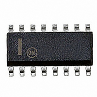
MC10SX1189DG ON Semiconductor, MC10SX1189DG Datasheet - Page 4

MC10SX1189DG
Manufacturer Part Number
MC10SX1189DG
Description
IC DRIVER COAX CABLE 16SOIC
Manufacturer
ON Semiconductor
Type
Driverr
Datasheet
1.MC10SX1189DR2G.pdf
(5 pages)
Specifications of MC10SX1189DG
Number Of Drivers/receivers
1/0
Voltage - Supply
4.5 V ~ 5.5 V
Mounting Type
Surface Mount
Package / Case
16-SOIC (3.9mm Width)
Supply Voltage (max)
5.5 V
Supply Voltage (min)
4.5 V
Maximum Operating Temperature
+ 85 C
Mounting Style
SMD/SMT
Minimum Operating Temperature
- 40 C
Device Type
Cable
Supply Voltage Range
4.5V To 5.5V
No. Of Pins
16
Operating Temperature Range
-40°C To +85°C
Filter Terminals
SMD
Logic Base Number
SX1189
Supply Voltage Min
4.5V
Rohs Compliant
Yes
Family Type
ECL
Input Type
2x ECL
Lead Free Status / RoHS Status
Lead free / RoHS Compliant
Protocol
-
Lead Free Status / Rohs Status
Lead free / RoHS Compliant
Other names
MC10SX1189DGOS
Available stocks
Company
Part Number
Manufacturer
Quantity
Price
Company:
Part Number:
MC10SX1189DG
Manufacturer:
ON Semiconductor
Quantity:
135
Part Number:
MC10SX1189DG
Manufacturer:
OM
Quantity:
20 000
NOTE: Device will meet the specifications after thermal equilibrium has been established when mounted in a test socket or printed circuit
5. V
6. The differential propagation delay is defined as the delay from the crossing points of the differential input signals to the crossing point of the
7. The single-ended propagation delay is defined as the delay from the 50% point of the input signal to the 50% point of the output signal.
8. Duty cycle skew is the difference between t
9. Minimum input swing for which AC parameters are guaranteed.
10. The CMR range is referenced to the most positive side of the differential input signal. Normal operation is obtained if the HIGH level falls
†For information on tape and reel specifications, including part orientation and tape sizes, please refer to our Tape and Reel Packaging
Table 3. AC CHARACTERISTICS
Symbol
ORDERING INFORMATION
Specifications Brochure, BRD8011/D.
t
t
t
t
t
t
t
V
V
MC10SX1189D
MC10SX1189DG
MC10SX1189DR2
MC10SX1189DR2G
PLH
PHL
r
f
r
f
skew
,
,
PP
CMR
differential output signals.
within the specified range and the peak-to-peak voltage lies between V
EE
,
board with maintained transverse airflow greater than 500 lfpm. Electrical parameters are guaranteed only over the declared
operating temperature range. Functional operation of the device exceeding these conditions is not implied. Device specification limit
values are applied individually under normal operating conditions and not valid simultaneously.
can vary +0.5 V to −0.5 V.
Propagation Delay
to Output
Propagation Delay
Rise Time
Fall Time
Rise Time
Fall Time
Within Device Skew
Minimum Input Swing
Common Mode Range
Device
Characteristic
DR → QR (Diff)
DR → QT (Diff)
DT → QT (Diff)
SEL → QT,QT
(V
CC
QR,QR
= 4.5 V to 5.5 V) (Note 5)
QT,QT
PLH
(SE)
(SE)
(SE)
and t
PHL
3.00
Min
175
150
250
225
225
200
450
100
100
150
150
200
http://onsemi.com
propagation delay through a device.
(Pb−Free)
(Pb−Free)
SOIC−16
SOIC−16
SOIC−16
SOIC−16
Package
−40°C
Typ
300
300
425
425
400
400
600
275
275
300
300
15
4
PP Min
1000
Max
4.35
450
500
650
700
650
725
850
400
400
550
550
and 1.0 V.
3.00
Min
225
175
300
250
275
225
500
125
125
150
150
200
0 to 85°C
Typ
325
325
450
450
425
425
650
275
275
300
300
15
2500 / Tape & Reel
2500 / Tape & Reel
1000
Max
4.35
500
550
650
700
650
725
800
400
400
550
550
45 Units / Rail
45 Units / Rail
Shipping
Unit
mV
ps
ps
ps
ps
V
†
Note 6
Note 7
1.5V to 50% Pt
20% to 80%
80% to 20%
20% to 80%
80% to 20%
Note 8
Note 9
Note 10
Condition


