CDB1601-120W-Z Cirrus Logic Inc, CDB1601-120W-Z Datasheet - Page 3
CDB1601-120W-Z
Manufacturer Part Number
CDB1601-120W-Z
Description
High-efficiency PFC Demo. Board
Manufacturer
Cirrus Logic Inc
Series
-r
Datasheets
1.CDB150X-01-Z.pdf
(2 pages)
2.CDB1601-120W-Z.pdf
(24 pages)
3.CDB1601-120W-Z.pdf
(16 pages)
Specifications of CDB1601-120W-Z
Silicon Manufacturer
Cirrus Logic
Kit Application Type
Power Management
Application Sub Type
Power Factor Correction (PFC)
Kit Contents
Board, Datasheet
Design Resources
CS150x/160x PCB Layout Guidelines
Featured Product
CS1501/CS1601 Power Factor Correction IC Controllers
Main Purpose
Power Management, Power Factor Correction
Embedded
No
Utilized Ic / Part
CS1601
Primary Attributes
108 ~ 305 VAC Input, 460V 120W Output
Secondary Attributes
Ballast Control, Up to 2 T5 Lamps
Lead Free Status / Rohs Status
Lead free / RoHS Compliant


1. INTRODUCTION
The CS1601 is a high-performance Variable Frequency Discontinuous Conduction Mode (VF-DCM), ac-
tive Power Factor Correction (PFC) controller, optimized to deliver the lowest PFC system cost for elec-
tronic ballast applications
and near unity power factor over a wide input voltage range (108-305 VAC).
The CS1601 uses an adaptive digital control algorithm. Both the ON time and the switching frequency are
varied on a cycle-by-cycle basis over the entire AC line to achieve close to unity power factor. The varia-
tion in switching frequency also provides a spread frequency spectrum, thus minimizing the conducted
EMI filtering requirements.
The feedback loop is closed through an integrated digital control system within the IC. Protection features
such as overvoltage, overcurrent, overpower, open circuit, overtemperature, and brownout help protect
the device during abnormal transient conditions. Details of these features are provided in the CS1601 data
sheet.
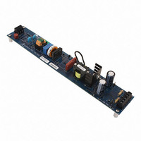
The CDB1601-120W board demonstrates the performance of the CS1601 over a wide input voltage range
of 108 to 305 VAC, typically seen in universal input ballast applications. This board has been designed
for a 460 V, 115 W full load output application.
Extreme caution needs to be exercised while handling this board. This board is to be powered up by
trained professionals only.
Prior to applying AC power to the CDB1601-120W board, the CS1601 needs to be biased using an exter-
nal 13 VDC power supply, applied across pins 1 and 3 of terminal block J5. Terminal block J6 is used to
connect the AC line. The load is connected to J7. As a safety measure, jumper J1 is provided as a means
to apply a small resistive load (200 kΩ minium) to rapidly discharge the output capacitors. Other jumpers
and test points are provided to evaluate the behavior of the IC and the various sections of the design.
DS931DB3
AC Line
Input
J6
The end product should use tar pitch or an equivalent compound for this purpose.
For lab evaluation purposes, a fan is recommended to provide adequate cooling.
ONLY QUALIFIED PERSONNEL SHOULD HANDLE THE CDB1601-120W.
.
The CS1601 uses a digital control algorithm that is optimized for high efficiency
Heatsinking is required for Q4.
Figure 1. Board Connections
High Voltage Hazard
WARNING:
DANGER
CDB1601-120W
J1
J7
J5
Terminals
V
Output
DD
Input
3
Related parts for CDB1601-120W-Z
Image
Part Number
Description
Manufacturer
Datasheet
Request
R

Part Number:
Description:
Development Kit
Manufacturer:
Cirrus Logic Inc
Datasheet:
Part Number:
Description:
Development Kit
Manufacturer:
Cirrus Logic Inc
Datasheet:


Part Number:
Description:
High-efficiency PFC + Fluorescent Lamp Driver Reference Design
Manufacturer:
Cirrus Logic Inc
Datasheet:
Part Number:
Description:
Development Kit
Manufacturer:
Cirrus Logic Inc
Datasheet:
Part Number:
Description:
Development Kit
Manufacturer:
Cirrus Logic Inc
Datasheet:

Part Number:
Description:
Development Kit
Manufacturer:
Cirrus Logic Inc
Datasheet:
Part Number:
Description:
Development Kit
Manufacturer:
Cirrus Logic Inc
Datasheet:
Part Number:
Description:
Development Kit
Manufacturer:
Cirrus Logic Inc
Datasheet:
Part Number:
Description:
Development Kit
Manufacturer:
Cirrus Logic Inc
Datasheet:

Part Number:
Description:
EVALUATION BOARD FOR CS8427
Manufacturer:
Cirrus Logic Inc
Datasheet:

Part Number:
Description:
BOARD EVAL FOR CS8416 RCVR
Manufacturer:
Cirrus Logic Inc
Datasheet:

Part Number:
Description:
EVALUATION BOARD FOR CS8420
Manufacturer:
Cirrus Logic Inc
Datasheet:

Part Number:
Description:
KIT DEVELOPMENT EP9315 ARM9
Manufacturer:
Cirrus Logic Inc
Datasheet:

Part Number:
Description:
KIT DEVELOPMENT EP9302 ARM9
Manufacturer:
Cirrus Logic Inc
Datasheet: