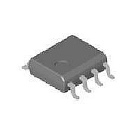
FDS86140 Fairchild Semiconductor, FDS86140 Datasheet - Page 2

FDS86140
Manufacturer Part Number
FDS86140
Description
MOSFET Power 100V N-Channel PowerTrench MOSFET
Manufacturer
Fairchild Semiconductor
Datasheet
1.FDS86140.pdf
(6 pages)
Specifications of FDS86140
Transistor Polarity
N-Channel
Resistance Drain-source Rds (on)
16 mOhms
Forward Transconductance Gfs (max / Min)
35 S
Drain-source Breakdown Voltage
100 V
Continuous Drain Current
11.2 A
Power Dissipation
5 W
Maximum Operating Temperature
+ 150 C
Mounting Style
SMD/SMT
Package / Case
SOIC-8
Lead Free Status / Rohs Status
Details
Available stocks
Company
Part Number
Manufacturer
Quantity
Price
Company:
Part Number:
FDS86140-NL
Manufacturer:
FAIRCHILD
Quantity:
12 604
©2011 Fairchild Semiconductor Corporation
FDS86140 Rev.C
Electrical Characteristics
Off Characteristics
On Characteristics
Dynamic Characteristics
Switching Characteristics
Drain-Source Diode Characteristics
NOTES:
1. R
2. Pulse Test: Pulse Width < 300 μs, Duty cycle < 2.0%.
3. Starting T
BV
ΔBV
I
I
V
r
g
C
C
C
R
t
t
t
t
Q
Q
Q
Q
V
t
Q
ΔV
DSS
GSS
d(on)
r
d(off)
f
rr
DS(on)
FS
GS(th)
SD
the user's board design.
ΔT
ΔT
iss
oss
rss
g
g
g
gs
gd
rr
Symbol
θJA
DSS
GS(th)
DSS
J
J
is determined with the device mounted on a 1 in
J
= 25 °C, L = 1 mH, I
Drain to Source Breakdown Voltage
Breakdown Voltage Temperature
Coefficient
Zero Gate Voltage Drain Current
Gate to Source Leakage Current
Gate to Source Threshold Voltage
Gate to Source Threshold Voltage
Temperature Coefficient
Static Drain to Source On Resistance
Forward Transconductance
Input Capacitance
Output Capacitance
Reverse Transfer Capacitance
Gate Resistance
Turn-On Delay Time
Rise Time
Turn-Off Delay Time
Fall Time
Total Gate Charge
Total Gate Charge
Gate to Source Charge
Gate to Drain “Miller” Charge
Source-Drain Diode Forward Voltage
Reverse Recovery Time
Reverse Recovery Charge
AS
= 23 A, V
Parameter
DD
a) 50 °C/W when mounted on a
= 90 V, V
1 in
2
2
T
pad 2 oz copper pad on a 1.5 x 1.5 in. board of FR-4 material. R
pad of 2 oz copper.
J
= 25 °C unless otherwise noted
GS
= 10 V.
V
V
V
V
V
f = 1 MHz
V
I
V
V
V
T
V
V
V
I
I
I
V
V
D
F
D
D
DD
GS
GS
GS
J
DS
GS
GS
GS
GS
DS
GS
GS
DS
GS
= 11.2 A, di/dt = 100 A/μs
= 250 μA, referenced to 25 °C
= 250 μA, V
= 250 μA, referenced to 25 °C
= 125 °C
= 50 V, V
= 50 V, I
= 10 V, R
= 0 V to 10 V
= 0 V to 5 V
= 10 V, I
= 0 V, I
= 0 V, I
= V
= 10 V, I
= 6 V, I
= 10 V, I
= 80 V, V
= ±20 V, V
2
DS
Test Conditions
, I
S
D
S
D
D
D
= 11.2 A
= 2 A
= 9 A
D
GS
GEN
GS
D
= 250 μA
GS
= 11.2 A,
= 11.2 A
DS
= 11.2 A,
= 11.2 A
= 0 V,
= 0 V
= 0 V
= 0 V
= 6 Ω
V
I
D
DD
= 11.2 A
= 50 V,
(Note 2)
(Note 2)
θJC
is guaranteed by design while R
b) 125 °C/W when mounted on a
Min
100
2
minimum pad.
1940
10.8
13.1
440
13.7
16.5
0.9
0.8
0.7
Typ
2.7
-11
8.1
5.6
4.8
8.0
6.5
59
20
53
35
23
29
70
2580
θCA
±100
Max
585
1.3
1.2
9.8
30
85
94
16
17
25
38
10
41
23
11
www.fairchildsemi.com
4
1
is determined by
mV/°C
mV/°C
Units
mΩ
pF
pF
pF
nC
nC
nC
ns
μA
nA
nC
nC
Ω
ns
ns
ns
ns
V
S
V
V


