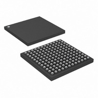
DS21Q48 Maxim Integrated Products, DS21Q48 Datasheet - Page 24

DS21Q48
Manufacturer Part Number
DS21Q48
Description
IC LIU E1/T1/J1 QUAD 5V 144-BGA
Manufacturer
Maxim Integrated Products
Type
Line Interface Units (LIUs)r
Specifications of DS21Q48
Protocol
E1
Voltage - Supply
4.75 V ~ 5.25 V
Mounting Type
Surface Mount
Package / Case
144-CSBGA
Lead Free Status / RoHS Status
Contains lead / RoHS non-compliant
Number Of Drivers/receivers
-
Available stocks
Company
Part Number
Manufacturer
Quantity
Price
DS2148/DS21Q48
3.2 Parallel Port Operation
When using the parallel interface on the DS2148 (BIS1 = 0) the user has the option for either multiplexed
bus operation (BIS1 = 0, BIS0 = 0) or nonmultiplexed bus operation (BIS1 = 0, BIS0 = 1). The DS2148
can operate with either Intel or Motorola bus timing configurations. If the PBTS pin is tied low, Intel
timing will be selected; if tied high, Motorola timing will be selected. All Motorola bus signals are listed
in parentheses. See the timing diagrams in Section
10
for more details.
3.3 Serial Port Operation
Setting BIS1 = 1 and BIS0 = 0 enables the serial bus interface on the DS2148. Port read/write timing is
unrelated to the system transmit and receive timing, allowing asynchronous reads or writes by the host.
See Section
10
for the AC timing of the serial port. All serial port accesses are LSB first. See
Figure
3-1,
Figure
3-2,
Figure
3-3, and
Figure 3-4
for more details.
Reading or writing to the internal registers requires writing one address/command byte prior to
transferring register data. The first bit written (LSB) of the address/command byte specifies whether the
access is a read (1) or a write (0). The next 5 bits identify the register address. Bit 7 is reserved and must
be set to 0 for proper operation.
The last bit (MSB) of the address/command byte is the burst mode bit. When the burst bit is enabled
(B = 1) and a READ operation is performed, addresses 0 through 15h are read sequentially, starting at
address 0h. And when the burst bit is enabled and a WRITE operation is performed, addresses 0 through
16h are written sequentially, starting at address 0h. Burst operation is stopped once address 15h is read.
See
Figure 3-5
and
Figure 3-6
for more details.
All data transfers are initiated by driving the CS input low. When input clock-edge select (ICES) is low,
input data is latched on the rising edge of SCLK and when ICES is high, input data is latched on the
falling edge of SCLK. When output clock-edge select (OCES) is low, data is output on the falling edge of
SCLK and when OCES is high, data is output on the rising edge of SCLK. Data is held until the next
falling or rising edge. All data transfers are terminated if the CS input transitions high. Port control logic
is disabled and SDO is tri-stated when CS is high.
24 of 73


