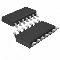
LT1030CS#TRPBF Linear Technology, LT1030CS#TRPBF Datasheet - Page 2

LT1030CS#TRPBF
Manufacturer Part Number
LT1030CS#TRPBF
Description
IC LINE DRVR LOWPWR QUAD 14-SOIC
Manufacturer
Linear Technology
Type
Line Driver, Transmitterr
Datasheet
1.LT1030CN.pdf
(4 pages)
Specifications of LT1030CS#TRPBF
Number Of Drivers/receivers
4/0
Protocol
RS232
Voltage - Supply
5 V ~ 15 V
Mounting Type
Surface Mount
Package / Case
14-SOIC (3.9mm Width), 14-SOL
Lead Free Status / RoHS Status
Lead free / RoHS Compliant
Available stocks
Company
Part Number
Manufacturer
Quantity
Price
ABSOLUTE
PARAMETER
Supply Current
Power Supply Leakage Current
Output Voltage Swing
Output Current
Output Overload Voltage (Forced)
Output Current
Input Overload Voltage (Forced)
Logic Input Levels
Logic Input Current
On/Off Pin Current
Slew Rate
PIN
V
LOGIC INPUT (Pins 2, 5, 9, 12): Operate properly on TTL
or CMOS levels. Output valid from (V
Connect to 5V when not used.
OUTPUT (Pins 3, 6, 8, 11): Line drive outputs.
ON/OFF (Pin 4): Shuts down entire circuit. Cannot be left
open. For “normally on” operation, connect between 5V to
10V.
GND (Pin 7): Ground must be more positive than V
LT1030
Supply Voltage ...................................................... ±15V
Logic Input Pins ............................................. V
On/Off Pin .................................................... GND to 12V
Output (Forced) .............................. V
Short-Circuit Duration (to ±30V) ..................... Indefinite
Operating Temperature Range
Storage Temperature ............................ – 65°C to 150°C
Lead Temperature (Soldering, 10 sec).................. 300°C
ELECTRICAL CHARACTERISTICS
The
temperature range.
2
–
Commercial ............................................. 0°C to 70°C
Guaranteed Functional by Design ....... – 25°C to 85°C
(Pin 1): Operates – 15V to – 2V.
U
●
denotes specifications which apply over the full operating
FUNCTIONS
U
W
MAXIMUM
U
W W
CONDITIONS
V
V
V
Load = 2mA
V
Operating or Shutdown
Shutdown
Operating or Shutdown
Low Input (V
High Input (V
V
V
0 ≤ V
ON/OFF
ON/OFF
ON/OFF
SUPPLY
IN
IN
> 2.0V
< 0.8V
IN
≤ 5V
≥ 2.4V, I
≤ 0.4V
≤ 0.1V
± 5V to ±15V
RATINGS
–
OUT
+ 2V) ≤ V
–
OUT
+ 30V, V
Positive
Negative
V
V
OUT
= High)
S
S
= Low)
= 0V, V
= ±15V, V
= 0, All Outputs Low
U
OUT
IN
–
+
OUT
to 25V
≤ 15V.
= ±30V
– 30V
(Supply Voltage = ±5 to ±15V)
–
= ± 20V
.
STROBE (Pin 13): Forces all outputs low. Drive with 3V.
V
Note: As with other bipolar ICs, forward biasing the substrate diode can cause
problems. The LT1030 will draw high current from V
circuited or pulled above ground. If this is possible, connecting a diode from V
ground will prevent the high current state. Any low cost diode can be used.
PACKAGE/ORDER
Consult factory for Industrial and Military grade parts.
Note 1: 3V applied to the Strobe pin will force all outputs low. Strobe pin
input impedance is about 2k to ground. Leave open when not used.
+
(–15V TO –5V)
(Pin 14): Positive supply 5V to 15V.
(0V TO 5V)
ON/OFF
14-LEAD PDIP
GND
●
●
●
●
●
●
●
N PACKAGE
T
T
V
JMAX
JMAX
–
1
2
3
4
5
6
7
= 125°C, θ
= 125°C, θ
V
14
1
V
+
TOP VIEW
+
MIN
–10
– 0.3V
– 30V
V
5
2
4
–
JA
JA
14-LEAD PLASTIC SO
= 90°C/ W (N)
= 95°C/ W (S)
S PACKAGE
14
13
12
11
10
9
8
LT1030
1N4001
V
(5V TO 15V)
STROBE
V
V
+
+
–
TYP
500
– 0.1V
+ 0.9V
1.4
1.4
10
12
10
30
15
1
2
2
2
INFORMATION
U
+
to ground if the V
LT1030 • PF01
V
V
–
MAX
–
ORDER PART
1000
8
7
150
100
100
+ 1.4V
0.8
10
15
20
20
65
30
W
+ 30V
LT1030CN
LT1030CS
LT1030CJ
CONSULT
FACTORY
NUMBER
–
pin is open
UNITS
U
V/µS
mA
–
µA
µA
µA
µA
µA
µA
µA
µA
to
V
V
V
V
V
V


