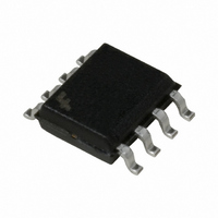
FIN1017M Fairchild Semiconductor, FIN1017M Datasheet

FIN1017M
Specifications of FIN1017M
Available stocks
Related parts for FIN1017M
FIN1017M Summary of contents
Page 1
... Meets or Exceeds the TIA/EIA-644 LVDS Standard Flow-Through Pinout Simplifies PCB Layout 8-Lead SOIC and US8 Packages Save Space Ordering Information Operating Part Number Temperature Range FIN1017MX -40 to +85°C FIN1017K8X -40 to +85°C © 2001 Fairchild Semiconductor Corporation FIN1017 • Rev. 1.0.3 Description ...
Page 2
... Pin# SOIC Function Table Input D IN LOW HIGH OPEN © 2001 Fairchild Semiconductor Corporation FIN1017 • Rev. 1.0.3 Figure 2. US-8 (Top View) Name D LVTTL Data Input IN D Non-inverting Driver Output OUT+ D Inverting Driver Output OUT- V Power Supply CC GND / GND Ground S NC ...
Page 3
... Fairchild does not recommend exceeding them or designing to Absolute Maximum Ratings. Symbol V Supply Voltage CC V Input Voltage IN T Operating Temperature A © 2001 Fairchild Semiconductor Corporation FIN1017 • Rev. 1.0.3 Parameter to GND Parameter 3 Min. Max. -0.5 +4.6 -0.5 +6.0 -0 ...
Page 4
... SK(PP) devices switching in the same direction (either LOW-to-HIGH or HIGH-to-LOW) when both devices operate with the same supply voltage, same temperature, and have identical test circuits. © 2001 Fairchild Semiconductor Corporation FIN1017 • Rev. 1.0.3 Conditions = 100 Ω, See Figure 3 ...
Page 5
... Figure 4. Differential Driver Propagation Delay and Transition Time Test Circuit Notes: Note A: All input pulses have frequency = 10MHz, t Note B: C includes all probe and fixture capacitances. L © 2001 Fairchild Semiconductor Corporation FIN1017 • Rev. 1.0.3 Figure 3. Differential Driver DC Test Circuit 2ns Figure 5 ...
Page 6
... Figure 6. Output High Voltage vs. Power Supply Voltage Figure 8. Output Short Circuit Current vs. Power Supply Voltage Figure 10. Differential Output Voltage vs. Load Resistor © 2001 Fairchild Semiconductor Corporation FIN1017 • Rev. 1.0.3 Figure 7. Output Low Voltage vs. Power Supply Voltage Figure 9. Differential Output Voltage vs. Power Supply Voltage Figure 11 ...
Page 7
... Typical Performance Characteristics Figure 12. Power Supply Current vs. Frequency Figure 14. Power Supply Current vs. Ambient Temperature Figure 16. Differential Propagation Delay vs. Ambient Temperature © 2001 Fairchild Semiconductor Corporation FIN1017 • Rev. 1.0.3 Figure 13. Power Supply Current vs. Power Supply Voltage Figure 15. Differential Propagation Delay vs. Power Supply Figure 17 ...
Page 8
... Typical Performance Characteristics Figure 18. Differential Pulse Skew (t vs. Ambient Temperature Figure 20. Transition Time vs. Ambient Temperature © 2001 Fairchild Semiconductor Corporation FIN1017 • Rev. 1.0 Figure 19. Transition Time PLH PHL vs. Power Supply Voltage 8 www.fairchildsemi.com ...
Page 9
... Package drawings are provided as a service to customers considering Fairchild components. Drawings may change in any manner without notice. Please note the revision and/or date on the drawing and contact a Fairchild Semiconductor representative to verify or obtain the most recent revision. Package specifications do not expand the terms of Fairchild’s worldwide terms and conditions, specifically the warranty therein, which covers Fairchild products. Always visit Fairchild Semiconductor’ ...
Page 10
... Package drawings are provided as a service to customers considering Fairchild components. Drawings may change in any manner without notice. Please note the revision and/or date on the drawing and contact a Fairchild Semiconductor representative to verify or obtain the most recent revision. Package specifications do not expand the terms of Fairchild’s worldwide terms and conditions, specifically the warranty therein, which covers Fairchild products. Always visit Fairchild Semiconductor’ ...
Page 11
... Fairchild Semiconductor Corporation FIN1017 • Rev. 1.0.3 11 www.fairchildsemi.com ...


