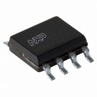
TJA1040T/N1,112 NXP Semiconductors, TJA1040T/N1,112 Datasheet - Page 7

TJA1040T/N1,112
Manufacturer Part Number
TJA1040T/N1,112
Description
IC CAN TRANSCEIVER HS 8-SOIC
Manufacturer
NXP Semiconductors
Type
Transceiverr
Datasheet
1.TJA1040TVM118.pdf
(17 pages)
Specifications of TJA1040T/N1,112
Package / Case
8-SOIC (3.9mm Width)
Number Of Drivers/receivers
1/1
Protocol
CAN
Voltage - Supply
4.75 V ~ 5.25 V
Mounting Type
Surface Mount
Product
Controller Area Network (CAN)
Number Of Transceivers
1
Data Rate
1 MBd
Supply Voltage (max)
5.25 V
Supply Voltage (min)
4.75 V
Supply Current (max)
70 mA
Maximum Operating Temperature
+ 150 C
Minimum Operating Temperature
- 40 C
Mounting Style
SMD/SMT
Lead Free Status / RoHS Status
Lead free / RoHS Compliant
Other names
935268735112
TJA1040TD
TJA1040TD
TJA1040TD
TJA1040TD
Philips Semiconductors
Note
1. All parameters are guaranteed over the virtual junction temperature range by design, but only 100% tested at 125 C
2003 Oct 14
V
I
I
V
V
I
R
R
R
C
C
Timing characteristics; see Fig.8
t
t
t
t
t
t
t
t
Thermal shutdown
T
O(sc)
O(reces)
LI
d(TXD-BUSon)
d(TXD-BUSoff)
d(BUSon-RXD)
d(BUSoff-RXD)
PD(TXD-RXD)
dom(TXD)
BUS
d(stb-norm)
j(sd)
O(reces)
dif(th)
hys(dif)
SYMBOL
i(cm)
i(cm)(m)
i(dif)
i(cm)
i(dif)
High speed CAN transceiver
ambient temperature for dies on wafer level, and in addition to this 100% tested at 25 C ambient temperature for
cased products; unless specified otherwise. For bare dies, all parameters are only guaranteed with the backside of
the die connected to ground.
recessive output voltage
short-circuit output current
recessive output current
differential receiver threshold
voltage
differential receiver hysteresis
voltage
input leakage current
common-mode input
resistance
common-mode input
resistance matching
differential input resistance
common-mode input
capacitance
differential input capacitance
delay TXD to bus active
delay TXD to bus inactive
delay bus active to RXD
delay bus inactive to RXD
propagation delay TXD to RXD V
TXD dominant time-out
dominant time for wake-up via
bus
delay standby mode to normal
mode
shutdown junction temperature
PARAMETER
normal mode; V
no load
standby mode; no load
V
normal mode;
V
V
standby or normal mode
V
standby or normal mode
V
V
normal mode
V
standby mode
normal mode
27 V < V
12 V < V
12 V < V
12 V < V
12 V < V
TXD
CC
CANH
CANH
TXD
TXD
STB
TXD
pin CANH; V
pin CANL; V
normal mode (see Fig.6) 0.5
standby mode
= 0 V;
= 0 V
= V
= V
= 0 V
= 0 V
CONDITIONS
= V
= V
CC
CC
CAN
CANL
CANH
CANL
CANH
CANL
CANL
7
; not tested
; not tested
< +32 V
CANL
CANH
< +12 V;
< +12 V;
< +12 V
< +12 V
TXD
= 5 V
= V
= 40 V 40
= 0 V
CC
;
2
0.4
50
15
25
25
10
15
35
40
300
0.75
5
155
0.1
40
2.5
5
3
MIN.
0.5V
0
70
0.7
0.7
70
0
25
0
50
70
50
65
100
600
1.75
7.5
165
70
TYP.
CC
Product specification
3
+0.1
100
+2.5
0.9
1.15
100
+5
35
+3
75
20
10
110
95
115
160
255
1000
5
10
180
95
MAX.
TJA1040
V
V
mA
mA
mA
V
V
mV
k
%
k
pF
pF
ns
ns
ns
ns
ns
UNIT
C
A
s
s
s


