DS90LV017M/NOPB National Semiconductor, DS90LV017M/NOPB Datasheet - Page 2
DS90LV017M/NOPB
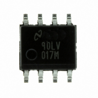
Manufacturer Part Number
DS90LV017M/NOPB
Description
IC DRIVER SINGLE HS DIFF 8-SOIC
Manufacturer
National Semiconductor
Type
Driverr
Datasheet
1.DS90LV017MNOPB.pdf
(4 pages)
Specifications of DS90LV017M/NOPB
Number Of Drivers/receivers
1/0
Protocol
RS644
Voltage - Supply
3 V ~ 3.6 V
Mounting Type
Surface Mount
Package / Case
8-SOIC (3.9mm Width)
Lead Free Status / RoHS Status
Lead free / RoHS Compliant
Other names
*DS90LV017M
*DS90LV017M/NOPB
DS90LV017M
*DS90LV017M/NOPB
DS90LV017M


www.national.com
DIFFERENTIAL DRIVER CHARACTERISTICS
V
∆V
V
V
V
∆V
I
I
I
V
V
I
I
V
I
Symbol
DIFFERENTIAL DRIVER CHARACTERISTICS
t
t
t
t
t
OZD
OXD
OSD
IH
IL
CC
PHLD
PLHD
SKD
TLH
THL
Symbol
OD
OH
OL
OS
IH
IL
CL
Absolute Maximum Ratings
If Military/Aerospace specified devices are required,
please contact the National Semiconductor Sales Office/
Distributors for availability and specifications.
Electrical Characteristics
Over Supply Voltage and Operating Temperature ranges, unless otherwise specified. (Notes 2, 3, 7)
Switching Characteristics
Over Supply Voltage and Operating Temperature Ranges, unless otherwise specified. (Notes 5, 6)
Note 1: “Absolute Maximum Ratings” are those values beyond which the safety of the device cannot be guaranteed. They are not meant to imply that the devices
should be operated at these limits. The table of “Electrical Characteristics” specifies conditions of device operation.
Note 2: Current into device pins is defined as positive. Current out of device pins is defined as negative. All voltages are referenced to ground except V
Note 3: All typicals are given for: V
Note 4: ESD Rating: HBM (1.5 kΩ, 100 pF) ≥ 4.5 kV
Note 5: C
Note 6: Generator waveform for all tests unless otherwise specified: f = 1 MHz, Z
Note 7: The DS90LV017 is a current mode device and only function with datasheet specification when a resistive load is applied to the drivers outputs.
Supply Voltage (V
Input Voltage (DI)
Output Voltage (DO
Maximum Package Power Dissipation
Derate M Package
Storage Temperature Range
OD
OS
M Package
L
Output Differential Voltage
V
Output High Voltage
Output Low Voltage
Offset Voltage
Offset Magnitude Change
TRI-STATE
Power-off Leakage
Output Short Circuit Current
Input High Voltage
Input Low Voltage
Input High Current
Input Low Current
Input Clamp Voltage
Power Supply Current
includes probe and fixture capacitance.
OD
Differential Propagation Delay High to Low
Differential Propagation Delay Low to High
Differential Skew |t
Transition Low to High Time
Transition High to Low Time
Magnitude Change
CC
Parameter
®
±
)
)
Leakage
Parameter
CC
PHLD
= +3.3V and T
9.5 mW/˚C above +25˚C
− t
−0.3V to (V
PLHD
@
−65˚C to +150˚C
+25˚C
R
V
V
V
V
I
No Load
R
|
CL
A
OUT
OUT
IN
IN
−0.3V to +3.9V
L
L
= +25˚C.
= 100Ω (Figure 1 )
= 100Ω
−0.3V to +6V
= −18 mA
= 3.6V or 2.4V
= GND or 0.5V
(Note 1)
= V
= 3.6V or GND, V
CC
1190 mW
+ 0.3V)
CC
or GND
Conditions
V
IN
R
(Figure 2 and Figure 3)
L
= V
2
= 100Ω, C
O
CC
CC
= 50Ω, t
Conditions
Recommended Operating
Conditions
Supply Voltage (V
Temperature (T
Lead Temperature Range
ESD Rating (Note 4)
or GND
= 0V
Soldering (4 sec.)
(HBM 1.5 kΩ, 100 pF)
r
L
≤ 6 ns, t
= 5 pF
f
≤ 6 ns (10%-90%).
A
)
DO+,
DO−
V
CC
Pin
DI
CC
)
Min
1.5
1.5
0
0
0
GND
−1.5
Min
250
Min
0.9
0.9
2.0
3.0
0
0
0
0
0
Typ
3.4
3.5
0.1
1
1
Typ
3.3
25
1.43
1.09
1.25
−0.8
Typ
340
4.5
10
±
±
−4
±
±
5
1
1
1
1
1
Max
Max
1.9
3.6
70
6
6
3
3
Max
450
±
±
V
±
±
1.6
1.6
0.8
35
25
−6
4
7
CC
10
10
10
10
≥ 4.5 kV
+260˚C
Units
OD
˚C
V
Units
Units
.
ns
ns
ns
ns
ns
mV
mV
mV
mA
mA
mA
µA
µA
µA
µA
V
V
V
V
V
V
Related parts for DS90LV017M/NOPB
Image
Part Number
Description
Manufacturer
Datasheet
Request
R

Part Number:
Description:
LVDS Single High Speed Differential Driver
Manufacturer:
National Semiconductor
Datasheet:
Part Number:
Description:
National Semiconductor [8-Bit D/A Converter]
Manufacturer:
National Semiconductor
Datasheet:
Part Number:
Description:
National Semiconductor [Media Coprocessor]
Manufacturer:
National Semiconductor
Datasheet:
Part Number:
Description:
Digitally Controlled Tone and Volume Circuit with Stereo Audio Power Amplifier, Microphone Preamp Stage and National 3D Sound
Manufacturer:
National Semiconductor
Datasheet:
Part Number:
Description:
Digitally Controlled Tone and Volume Circuit with Stereo Audio Power Amplifier, Microphone Preamp Stage and National 3D Sound
Manufacturer:
National Semiconductor
Datasheet:
Part Number:
Description:
AC97 Rev 2 Codec with Sample Rate Conversion and National 3D Sound
Manufacturer:
National Semiconductor
Part Number:
Description:
Manufacturer:
National Semiconductor
Datasheet:
Part Number:
Description:
Manufacturer:
National Semiconductor
Datasheet:
Part Number:
Description:
General Purpose, Low Voltage, Low Power, Rail-to-Rail Output Operational Amplifiers
Manufacturer:
National Semiconductor
Datasheet:
Part Number:
Description:
8-bit 20 MSPS flash A/D converter.
Manufacturer:
National Semiconductor
Datasheet:
Part Number:
Description:
Low Noise Quad Operational Amplifier
Manufacturer:
National Semiconductor
Datasheet:
Part Number:
Description:
Quad Differential Line Receivers
Manufacturer:
National Semiconductor
Datasheet:
Part Number:
Description:
Quad High Speed Trapezoidal? Bus Transceiver
Manufacturer:
National Semiconductor
Datasheet:
Part Number:
Description:
Dual Line Receiver
Manufacturer:
National Semiconductor
Datasheet: