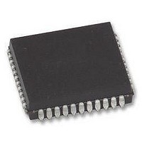
VRS51C1000-40-LG Ramtron, VRS51C1000-40-LG Datasheet - Page 6

VRS51C1000-40-LG
Manufacturer Part Number
VRS51C1000-40-LG
Description
Microcontrollers (MCU) 64K+1K 40MHz 5V
Manufacturer
Ramtron
Datasheet
1.VRS51C1000-40-PG.pdf
(48 pages)
Specifications of VRS51C1000-40-LG
Data Bus Width
8 bit
Program Memory Type
Flash
Program Memory Size
64 KB
Data Ram Size
1 KB
Interface Type
UART
Maximum Clock Frequency
40 MHz
Number Of Programmable I/os
36
Number Of Timers
3
Operating Supply Voltage
4.5 V to 5.5 V
Maximum Operating Temperature
+ 85 C
Mounting Style
SMD/SMT
Package / Case
PLCC-44
Minimum Operating Temperature
- 40 C
Lead Free Status / Rohs Status
Details
VRS51C1000 Program Memory
The VRS51C1000 includes 64KB of on-chip Flash
memory that can be used as program memory or as
general non-volatile data storage memory using the In-
Application Programming feature (IAP).
ISP Boot Program Memory Zone
The upper portion of the VRS51C1000 Flash memory
can be reserved to store an ISP (In-System
Programmable) boot loader program.
This boot program can be used to program the Flash
memory via the serial interface (or via any other
method)
Programming (IAP) feature of the VRS51C1000. This
allows the processor to load the program from an
external device or system, and program it into the
Flash memory (See the VRS51C1000 IAP feature
section)
The size of the memory block reserved for the ISP
boot loader program (when activated) is adjustable
from 512 Bytes up to 4K bytes in increments of 512
bytes.
F
Programming the ISP Boot Program
The ISP boot program must be programmed into the
device using a parallel programmer (such as the
VERSAMCU-PPR)
programmer that supports the VRS51C1000.
Flash memory reserved for the ISP program is defined
by the parallel programmer software at the moment the
device is programmed.
______________________________________________________________________________________________
www.ramtron.com
IGURE
VRS51C1000
ISP Config value x 512Bytes
3: VRS51C1000-ISP P
ISP Program Size =
by
making
ROGRAM SIZE VS
or
use
a
ISP C
of
commercial
ONFIG
the
. V
ALUE
In-Application
parallel
The
FFFFh
FE00h
FC00h
FA00h
F800h
F600h
F400h
F200h
F000h
0000h
When programming the ISP boot program into the
VRS51C1000, the “lock bit” option should be activated
in order to protect the ISP flash memory zone from
being inadvertently erased (can happen when the
Flash Erase operations are performed under the
control of the ISP boot program) or to prevent the
VRS51C1000 flash memory from being read back
using a parallel programmer.
If an Erase operation is performed using a parallel
programmer, the entire flash memory, including the
ISP Boot program memory zone will be erased.
ISP Program Start Conditions
Setting the ISP page configuration to a value other
than 0 will result in the Processor jumping to the base
address of the ISP boot code when a hardware reset is
performed (provided that the value FFh is present at
program address 0000h).
When the ISP page configuration is set to 0 at the
moment the device is programmed using a parallel
programmer, the ISP boot feature will be disabled.
page 6 of 48


