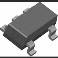
LMH6559MF National Semiconductor, LMH6559MF Datasheet - Page 14

LMH6559MF
Manufacturer Part Number
LMH6559MF
Description
IC, CLOSED LOOP BUFF SGL 1.75GHZ SOT23-5
Manufacturer
National Semiconductor
Datasheet
1.LMH6559MA.pdf
(22 pages)
Specifications of LMH6559MF
No. Of Amplifiers
1
Gain Bandwidth
1.75GHz
Slew Rate
4580V/µs
Supply Voltage Range
3V To 10V
Output Current
75mA
Amplifier Output
Single Ended
Operating Temperature Range
-40°C To +85°C
Rohs Compliant
No
Available stocks
Company
Part Number
Manufacturer
Quantity
Price
Part Number:
LMH6559MF
Manufacturer:
NS/国半
Quantity:
20 000
Company:
Part Number:
LMH6559MFX
Manufacturer:
NSC
Quantity:
3 400
www.national.com
Application Notes
Z
mensions of the pcb line, such as pcb thickness, width of the
trace and e
transmission line theory for calculating Z
e
h pcb height
W trace width
th thickness of the copper
If we ignore the thickness of the copper in comparison to the
width of the trace then we have the following equation:
With this formula it is possible to calculate the line imped-
ance vs. the trace width. Figure 5 shows the impedance
associated with a given line width. Using the same formula it
is also possible to calculate what happens when e
over a certain range of values. Varying the e
1 to 10 gives a variation for the Characteristic Impedance of
about 40Ω from 80Ω to 38Ω. Most transmission lines are
designed to have 50Ω or 75Ω impedance. The reason for
that is that in many cases the pcb trace has to connect to a
cable whose impedance is either 50Ω or 75Ω. As shown e
and the line width influence this value.
r
0
can be calculated by knowing some of the physical di-
relative dielectric constant
r
, relative dielectric constant. The formula given in
FIGURE 4.
(Continued)
0
is as follows:
r
over a range of
20064139
r
varies
(1)
(2)
r
14
Next, there will be a discussion of some issues associated
with the interaction of the transmission line at the source and
at the load.
Connecting A Load Using A Transmission Line
In most cases, it is unrealistic to think that we can place a
driver or buffer so close to the load that we don’t need a
transmission line to transport the signal. The pcb trace
length between a driver and the load may affect operation
depending upon the operating frequency. Sometimes it is
possible to do measurements by connecting the DUT directly
to the analyzer. As frequencies become higher the short
lines from the DUT to the analyzer become long lines. When
this happens there is a need to use transmission lines. The
next point to examine is what happens when the load is
connected to the transmission line. When driving a load, it is
important to match the line and load impedance, otherwise
reflections will occur and this phenomena will distort the
signal. If a transient is applied at T = 0 (Figure 6, trace A) the
resultant waveform may be observed at the start point of the
transmission line. At this point (begin) on the transmission
line the voltage increases to (V) and the wave front travels
along the transmission line and arrives at the load at T = 10.
At any point across along the line I = V/Z
impedance of the transmission line. For an applied transient
of 2V with Z
is 40mA. Many vintage opamps cannot deliver this level of
current because of an output current limitation of about
20mA or even less. At T = 10 the wave front arrives at the
load. Since the load is perfectly matched to the transmission
line all of the current traveling across the line will be ab-
sorbed and there will be no reflections. In this case source
and load voltages are exactly the same. When the load and
the transmission line have unequal values of impedance a
different situation results. Remember there is another basic
which says that energy cannot be lost. The power in the
transmission line is P = V
is 2
power of 80mW arrives at the 75Ω load and causes a
voltage of the proper amplitude to maintain the incoming
power.
2
/50 = 80mW. Assume a load of 75Ω. In that case a
0
= 50Ω the current from the buffer output stage
FIGURE 5.
2
/R. In our example the total power
0
, where Z
20064142
0
is the


