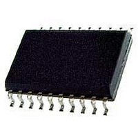
MC100LVEL17DWR2 ON Semiconductor, MC100LVEL17DWR2 Datasheet

MC100LVEL17DWR2
Manufacturer Part Number
MC100LVEL17DWR2
Description
Buffers & Line Drivers 3.3V ECL Quad Diff
Manufacturer
ON Semiconductor
Specifications of MC100LVEL17DWR2
Logic Family
100LV
Logic Type
ECL Quad Differential Receiver
Supply Voltage (max)
- 3.8 V, 3.8 V
Supply Voltage (min)
- 3 V, 3 V
Maximum Operating Temperature
+ 85 C
Mounting Style
SMD/SMT
Package / Case
SO-20 WB
Minimum Operating Temperature
- 40 C
Number Of Lines (input / Output)
/ /
Supply Current
33 mA
Lead Free Status / Rohs Status
No RoHS Version Available
Available stocks
Company
Part Number
Manufacturer
Quantity
Price
Company:
Part Number:
MC100LVEL17DWR2
Manufacturer:
ON
Quantity:
5 510
Company:
Part Number:
MC100LVEL17DWR2
Manufacturer:
NXP
Quantity:
5 510
Part Number:
MC100LVEL17DWR2
Manufacturer:
ON
Quantity:
20 000
MC100LVEL17
3.3V ECL Quad Differential
Receiver
Description
device is functionally equivalent to the E116 device with the capability
of operation from either a −3.3 V or +3.3 V supply voltage.
and the D input will be pulled down to V
the Q output LOW and ensure stability.
this device only. For single-ended input conditions, the unused
differential input is connected to V
V
and V
to 0.5 mA. When not used, V
Features
•
•
•
•
•
•
•
•
*For additional information on our Pb−Free strategy and soldering details, please
© Semiconductor Components Industries, LLC, 2006
November, 2006 − Rev. 7
download the ON Semiconductor Soldering and Mounting Techniques
Reference Manual, SOLDERRM/D.
BB
The MC100LVEL17 is a 3.3 V ECL, quad differential receiver. The
Under open input conditions, the D input will be biased at V
The V
with V
with V
Pullup and Pulldown on D Inputs
325 ps Propagation Delay
High Bandwidth Output Transitions
The 100 Series Contains Temperature Compensation
PECL Mode Operating Range: V
NECL Mode Operating Range: V
Internal Input Pulldown Resistors D Inputs;
Q Output will Default LOW with Inputs Open or at V
Pb−Free Packages are Available*
may also rebias AC coupled inputs. When used, decouple V
CC
BB
via a 0.01 mF capacitor and limit current sourcing or sinking
EE
EE
pin, an internally generated voltage supply, is available to
= −3.0 V to −3.8 V
= 0 V
BB
should be left open.
BB
CC
CC
as a switching reference voltage.
= 3.0 V to 3.8 V
= 0 V
EE
. This operation will force
EE
1
CC
BB
/2
*For additional marking information, refer to
See detailed ordering and shipping information in the package
dimensions section on page 5 of this data sheet.
Application Note AND8002/D.
ORDERING INFORMATION
20
A
WL
YY
WW
G
1
MARKING DIAGRAM*
http://onsemi.com
= Assembly Location
= Wafer Lot
= Year
= Work Week
= Pb−Free Package
AWLYYWWG
DW SUFFIX
CASE 751D
SO−20 WB
100LVEL17
Publication Order Number:
MC100LVEL17/D


