NLSF3T125MNR2 ON Semiconductor, NLSF3T125MNR2 Datasheet
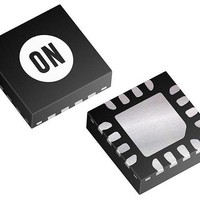
Buffers & Line Drivers 2-5.5V Quad Bus

NLSF3T125MNR2

Manufacturer Part Number
NLSF3T125MNR2
Description
Buffers & Line Drivers 2-5.5V Quad Bus
Manufacturer
ON Semiconductor
Datasheet

Specifications of NLSF3T125MNR2

Logic Family
NLSF
Logic Type
CMOS
Number Of Channels Per Chip
4
Polarity
Non-Inverting
Supply Voltage (max)
5.5 V
Supply Voltage (min)
2 V
Maximum Operating Temperature
+ 85 C
Mounting Style
SMD/SMT
Package / Case
QFN-16
High Level Output Current
- 8 mA
Low Level Output Current
8 mA
Maximum Power Dissipation
500 mW
Minimum Operating Temperature
- 40 C
Number Of Lines (input / Output)
4 / 3
Output Type
3-State
Propagation Delay Time
11.5 ns at 3.3 V
Lead Free Status / Rohs Status
No RoHS Version Available

Available stocks

Company
Part Number
Manufacturer
Quantity
Price
Part Number:
NLSF3T125MNR2
Manufacturer:
MIC
Quantity:
200
Part Number:
NLSF3T125MNR2G
Manufacturer:
SWITCHCOR
Quantity:
108
NLSF3T125
Quad Bus Buffer
with 3−State Control Inputs
with silicon gate CMOS technology. It achieves high speed operation
similar to equivalent Bipolar Schottky TTL while maintaining CMOS
low power dissipation.
High to place the output into the high impedance state.
used as a level converter for interfacing 3.3 V to 5.0 V, because it has
full 5.0 V CMOS level output swings.
between 0 V and 5.5 V are applied, regardless of the supply voltage.
The output structures also provide protection when V
input and output structures help prevent device destruction caused by
supply voltage − input/output voltage mismatch, battery backup, hot
insertion, etc.
output which provides high noise immunity and stable output. The
inputs tolerate voltages up to 7.0 V, allowing the interface of 5.0 V
systems to 3.0 V systems.
March, 2004 − Rev. 2
The NLSF3T125 is a high speed CMOS quad bus buffer fabricated
The NLSF3T125 requires the 3−state control input (OE) to be set
The T125 inputs are compatible with TTL levels. This device can be
The NLSF3T125 input structures provide protection when voltages
The internal circuit is composed of three stages, including a buffer
High Speed: t
Low Power Dissipation: I
TTL−Compatible Inputs: V
Power Down Protection Provided on Inputs
Balanced Propagation Delays
Designed for 2.0 V to 5.5 V Operating Range
Low Noise: V
Pin and Function Compatible with Other Standard Logic Families
Latchup Performance Exceeds 300 mA
ESD Performance: Human Body Model; > 2000 V,
Chip Complexity: 72 FETs or 18 Equivalent Gates
Semiconductor Components Industries, LLC, 2004
OE1
OE2
OE3
OE4
A1
A2
A3
A4
Active−Low Output Enables
Figure 1. Logic Diagram
16
15
12
13
4
3
9
8
PD
OLP
= 3.8 ns (Typ) at V
= 0.8 V (Max)
Machine Model; > 200 V
10
1
5
7
CC
IL
= 4.0 mA (Max) at T
= 0.8 V; V
Y1
Y2
Y3
Y4
CC
= 5.0 V
FUNCTION TABLE
IH
A
H
X
L
Inputs
= 2.0 V
NLSF3T125
OE
H
L
L
A
CC
Output
= 25 C
H
Y
L
Z
= 0 V. These
1
†For information on tape and reel specifications,
NLSF3T125MNR2
including part orientation and tape sizes, please
refer to our Tape and Reel Packaging Specifications
Brochure, BRD8011/D.
Device
.
ORDERING INFORMATION
A
WL = Wafer Lot
Y
WW = Work Week
http://onsemi.com
1
= Assembly Location
= Year
CASE 485G
MARKING
DIAGRAM
16
(Top View)
QFN−16
ALYW
XXX
Package
QFN−16
Publication Order Number:
Tape & Reel
NLSF3T125/D
3000 Units/
Shipping†

Related parts for NLSF3T125MNR2

NLSF3T125MNR2 Summary of contents

Page 1

... Y = Year WW = Work Week ORDERING INFORMATION Device Package Shipping† 3000 Units/ NLSF3T125MNR2 QFN−16 Tape & Reel †For information on tape and reel specifications, including part orientation and tape sizes, please refer to our Tape and Reel Packaging Specifications Brochure, BRD8011/D. . Publication Order Number: ...

Page 2

MAXIMUM RATINGS Î Î Î Î Î Î Î Î Î Î Î Î Î Î Î ...

Page 3

DC ELECTRICAL CHARACTERISTICS Î Î Î Î ...

Page 4

AC ELECTRICAL CHARACTERISTICS Î Î Î Î ...

Page 5

NOISE CHARACTERISTICS (Input Symbol V Quiet Output Maximum Dynamic V OLP V Quiet Output Minimum Dynamic V OLV V Minimum High Level Dynamic Input Voltage IHD V Maximum Low Level Dynamic Input Voltage ILD NLSF3T125 = ...

Page 6

PHL PLH 1.5V Y Figure 3. TEST POINT OUTPUT DEVICE UNDER TEST *Includes all probe and jig capacitance Figure 5. Test Circuit NLSF3T125 SWITCHING WAVEFORMS OE 1.5V 3.0V GND 1. ...

Page 7

... EXPOSED PAD 3.25 E2 0.128 e *For additional information on our Pb−Free strategy and soldering details, please download the ON Semiconductor Soldering and Mounting Techniques Reference Manual, SOLDERRM/D. http://onsemi.com 7 ASME Y14.5M, 1994. TERMINAL AND IS MEASURED BETWEEN 0.25 AND 0.30 MM FROM TERMINAL. PAD AS WELL AS THE TERMINALS. ...

Page 8

... Fax: 303−675−2176 or 800−344−3867 Toll Free USA/Canada Email: orderlit@onsemi.com NLSF3T125 N. American Technical Support: 800−282−9855 Toll Free USA/Canada Japan: ON Semiconductor, Japan Customer Focus Center 2−9−1 Kamimeguro, Meguro−ku, Tokyo, Japan 153−0051 Phone: 81−3−5773−3850 http://onsemi.com 8 ON Semiconductor Website: http://onsemi ...

Related keywords