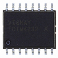
TOIM4232-TR3 Vishay, TOIM4232-TR3 Datasheet - Page 12

TOIM4232-TR3
Manufacturer Part Number
TOIM4232-TR3
Description
IC SIR ENDEC IRDA 115.2K 16-SOIC
Manufacturer
Vishay
Type
Infrared Encoder/Decoderr
Datasheet
1.TOIM4232-TR3.pdf
(17 pages)
Specifications of TOIM4232-TR3
Voltage - Supply, Analog
2.7 V ~ 3.6 V
Voltage - Supply, Digital
2.7 V ~ 3.6 V
Mounting Type
Surface Mount
Package / Case
16-SOIC (0.300", 7.5mm Width)
Data Transmission Rate
2.4 Kbits/s to 115.2 Kbits/s
Mounting Style
SMD/SMT
Operating Voltage
2.7 V to 3.6 V
Maximum Operating Temperature
+ 85 C
Minimum Operating Temperature
- 25 C
Ic Function
SIR Endec For IrDA Application
Brief Features
Pulse Shaping Function, Programmable Baud Clock Generator, Low Operating Current
Supply Voltage Range
2.7V To 3.6V
Operating Temperature (min)
-25C
Operating Temperature Classification
Commercial
Operating Temperature (max)
85C
Package Type
SOIC
Rad Hardened
No
Lead Free Status / RoHS Status
Lead free / RoHS Compliant
Applications
-
Lead Free Status / Rohs Status
Compliant
Other names
751-1200-2
Available stocks
Company
Part Number
Manufacturer
Quantity
Price
Company:
Part Number:
TOIM4232-TR3
Manufacturer:
Vishay Semiconductors
Quantity:
135
Company:
Part Number:
TOIM4232-TR3
Manufacturer:
MICREL
Quantity:
442
Part Number:
TOIM4232-TR3
Manufacturer:
VISHAY/威世
Quantity:
20 000
TOIM4232
Vishay Semiconductors
TOIM4232 (TOIM5232) ENCODER - DECODER INTERFACE
PROGRAMMING AND DATA TRANSMISSION
Operation and programming of the TOIM4232 and
TOIM5232 interface devices are described below. Figure 4
shows the basic circuit design with 3 blocks: the RS232 to
3 V logic level shifter, the encoder/decoder (endec) circuit
and the transceiver to build a dongle for RS232 IrDA
CIRCUIT DESCRIPTION
This circuit demonstrates the operation of an SIR IrDA
transceiver module. The transceiver U3 (e.g., as shown the
TFDU4101 or TFDU4300 or any other) converts the digital
electrical input signal to an optical output signal to be
transmitted, receives the optical signal, and converts these
to electrical digital signals. While the IrDA physical layer
protocol transmits only the “0” represented by a pulse with a
“Return to Zero Inverted (RZI)” logic, the RS232 protocol
needs a “No Return to Zero (NRZ)” representation. This
decoding/encoding process is done by U2, an interface
circuit stretching the received pulses and shortening the
pulses to be transmitted according to the IrDA physical layer
conditions. U1 interfaces the RS232 logic bipolar levels to
the 3 V logic of the endec U2. The board is connected by
CON9 to the RS232 port (of a computer or other equipment.
The basic IrDA transmission speed is 9600 bit/s. This is the
default state of the endec in power-on condition. Also,
activating the reset line at pin 1 (18) will set the device to this
basic state.
Note: The first pin number refers to TOIM4232; the second
number in brackets refers to TOIM5232. The crystal Y1
controls the timing of the endec as a clock reference. The
outputs S1 and S2 are programmable outputs for control
operations and the outputs RD_LED and TD_LED can drive
LEDs for indicating data flow.
www.vishay.com
12
CON9
J1
1
6
2
7
3
8
4
9
5
External input
3.6V max.
RXD
TXD
Vcc
C3
C4
+
+
RTS (BR/D)
DTR (RESET)
CON2
11
10
12
J2
1
3
4
5
9
1
2
C+
C1-
C2+
C2-
T1IN
T2IN
R1OUT
R2OUT
MAX3232
U1
irdasupportAM@vishay.com, irdasupportAP@vishay.com,
C1
T1OUT
T2OUT
For technical questions within your region, please contact one of the following:
R1IN
R2IN
GND
VCC
+
V+
V-
C2
16
2
6
15
14
7
13
8
+
C6
+
R1
C5
SIR Endec for IrDA
+
C7
Fig. 4 - Circuit Diagram of the Demo Board
Integrated Interface Circuit
Z2
C8
Y1
R2
1(18)
2(19)
7(5)
4(2)
5(3)
6(4)
8(7)
3(1)
C9
(TOIM5232)
RESET
BR/D
RD_232
TD_232
Vcc_SD
X1
X2
GND
TOIM4232
*) (6), (8), (11), (15), (20)
®
extension. U1 is the level shifter to convert the RS232 logic
levels to unipolar
Interface (endec) converting the NRZ - RS232 logic to IrDA
RZI -
IrDA-compliant optical signals.
PROGRAMMING THE ENDEC
For decoding data rates other than the default, the endec is
to be programmed to set the internal counters and timers. To
switch the endec from the data transfer mode to the bit rate
programming mode, the input BR/D, pin 2 (19) is set active
high (BR/D = “1”). In this case the TOIM5232 interprets the
7 LSBs at the TD_232 input as a control word. The operating
bit rate will change to its supposedly new rate when the BR/D
returns back to low (“0”). Set the UART to 8 bit, no parity, 1
stop bit.
The control byte consists of 8 bit after the start bit (STA,
which is “0”). Keep in mind that the order is LSB first, MSB
last.
The diagram in figure 5 shows the programming byte
“0-1010-1100” in the order
STA, B0, B1, B2, B3, S0, S1, S2, X. This order is from right
to left in table 1. B0 is sent first as LSB (see figure 5).
The four least significant bits are responsible for the data rate
according to table 2 while the four higher bits are for setting
the IrDA pulse duration (S0), and the two outputs of the
Endec S1 and S2. Bit 8 is not used.
U2
Applications
RD_LED
TD_LED
RD_IR
TD_IR
Vcc
NC
S2
S1
logic. The transceiver U3 transmits and receives
16(17)
13(13)
12(12)
10(10)
15(16)
14(14)
11 *)
9(9)
irdasupportEU@vishay.com
3 V logic; U2 is the encoder/decoder
C10
C11
+
R3
This line not used fot TFDU4101
2
4
6
8
TFDU4101
TFDU4300
Cathode
RXD
Vcc1
GND
IRED
Document Number: 82546
TFDU4300:Vlog
TFDU4101:NC
U3
Anode
IRED
Rev. 2.1, 17-Nov-10
TXD
21046
SD
.
1
3
5
7
R4
optional


