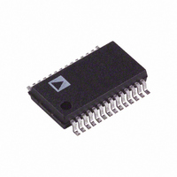
AD1896AYRSZ Analog Devices Inc, AD1896AYRSZ Datasheet - Page 24

AD1896AYRSZ
Manufacturer Part Number
AD1896AYRSZ
Description
IC CONV SAMPLE RATE ASYNC 28SSOP
Manufacturer
Analog Devices Inc
Type
Sample Rate Converterr
Datasheet
1.AD1896AYRSZ.pdf
(28 pages)
Specifications of AD1896AYRSZ
Applications
Automotive Audio, processing, receivers
Voltage - Supply, Digital
3.13 V ~ 3.46 V
Mounting Type
Surface Mount
Package / Case
28-SSOP
Audio Control Type
Sample Rate Converter
Output Power
132mW
Supply Voltage Range
3.135V To 3.465V, 3.135V To 5.5V
Operating Temperature Range
-40°C To +105°C
Audio Ic Case Style
SSOP
Lead Free Status / RoHS Status
Lead free / RoHS Compliant
Voltage - Supply, Analog
-
Lead Free Status / RoHS Status
Lead free / RoHS Compliant, Lead free / RoHS Compliant
Available stocks
Company
Part Number
Manufacturer
Quantity
Price
Company:
Part Number:
AD1896AYRSZRL
Manufacturer:
CYPRESS
Quantity:
92
AD1896
MATCHED-PHASE MODE (NON-TDM MODE) APPLICATION
Serial Data Port Master Clock Modes
Either of the AD1896 serial ports can be configured as a master
serial data port. However, only one serial port can be a master
while the other has to be a slave. In master mode, the AD1896
requires a 256 ¥ f
For a maximum master clock frequency of 30 MHz, the maxi-
mum sample rate is limited to 96 kHz. In slave mode, sample
rates up to 192 kHz can be handled.
When either of the serial ports is operated in master mode, the
master clock is divided down to derive the associated left/
right subframe clock (LRCLK) and serial bit clock (SCLK).
The master clock frequency can be selected for 256, 512, or 768
times the input or output sample rate. Both the input and out-
put serial ports will support master mode LRCLK and SCLK
generation for all serial modes, left justified, I
TDM for the output serial port.
LRCLK
SCLK
I
I
(f
S_IN
)
TDM_IN
M2
CLOCK-MASTER
PHASE-MASTER
0
S
AD1896
, 512 ¥ f
Figure 12. Daisy-Chain Configuration for TDM Mode (First AD1896 Being Clock-Master)
TDM_IN
SDATA_I
LRCLK_I
SCLK_I
MCLK
RESET
PHASE-MASTER
AND
M1
M2 M1 M0
0
1
AD1896
LRCLK_O
SDATA_O
SCLK_O
0
LRCLK_O
SDATA_O
S
M0
SCLK_O
, or 768 ¥ f
1
0
Figure 13. Typical Configuration for Matched-Phase Mode Operation
S
master clock (MCLK_I).
2
S, right justified, and
TDM_IN
TDM_IN
SDATA_I
LRCLK_I
SCLK_I
MCLK
RESET
M2
0
1
M2 M1 M0
1
AD1896
AD1896
SLAVE1
SLAVE-1
0
M1
LRCLK_O
SDATA_O
0
0
SCLK_O
LRCLK_O
SDATA_O
0
SCLK_O
M0
0
0
–24–
MMODE_0/
MMODE_1/
MMODE_2
2
0
0
0
0
1
1
1
1
TDM_IN
SDATA_I
LRCLK_I
SCLK_I
MCLK
RESET
M2 M1 M0
1
AD1896
1
0
0
1
1
0
0
1
1
SLAVE2
TDM_IN
M2
0
0
1
LRCLK_O
SDATA_O
SCLK_O
AD1896
SLAVE-n
Table IV. Serial Data Port Clock Modes
0
0
0
1
0
1
0
1
0
1
M1
0
0
LRCLK_O
SDATA_O
SCLK_O
Interface Format
Both serial ports are in slave mode.
Output serial port is master with 768 ¥ f
Output serial port is master with 512 ¥ f
Output serial port is master with 256 ¥ f
Matched-phase Mode
Input serial port is master with 768 ¥ f
Input serial port is master with 512 ¥ f
Input serial port is master with 256 ¥ f
M0
0
0
TDM_IN
SDATA_I
LRCLK_I
SCLK_I
MCLK
RESET
STANDARD MODE
MATCHED-PHASE MODE
M2 M1 M0
1
AD1896
SLAVEn
0
LRCLK_O
SDATA_O
SCLK_O
DR0
RFS0
RCLK0
0
SHARC
DSP
SDOm
SDO1
SDO2
SDOn
LRCLK
SCLK
MCLK
RESET
O
O
(64f
REV. A
S_OUT
S_OUT
(f
S_OUT
S_IN
S_IN
S_IN
S_OUT
S_OUT
.
.
.
)
.
.
.
)


