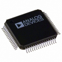
ADV7301AKST Analog Devices Inc, ADV7301AKST Datasheet - Page 50

ADV7301AKST
Manufacturer Part Number
ADV7301AKST
Description
IC DAC VIDEO HDTV 6-12BIT 64LQFP
Manufacturer
Analog Devices Inc
Type
Video Encoderr
Datasheet
1.ADV7301AKST.pdf
(68 pages)
Specifications of ADV7301AKST
Rohs Status
RoHS non-compliant
Applications
DVD, Set-Top Boxes
Voltage - Supply, Analog
2.37 V ~ 2.63 V
Voltage - Supply, Digital
2.37 V ~ 3.6 V
Mounting Type
Surface Mount
Package / Case
64-LQFP
Number Of Dac's
6
Adc/dac Resolution
12b
Screening Level
Commercial
Package Type
LQFP
Pin Count
64
Lead Free Status / RoHS Status
Compliant
Available stocks
Company
Part Number
Manufacturer
Quantity
Price
Company:
Part Number:
ADV7301AKST
Manufacturer:
AD
Quantity:
433
Company:
Part Number:
ADV7301AKST
Manufacturer:
ADI
Quantity:
300
Company:
Part Number:
ADV7301AKST
Manufacturer:
Analog Devices Inc
Quantity:
10 000
Part Number:
ADV7301AKSTZ
Manufacturer:
ADI/亚德诺
Quantity:
20 000
ADV7300A/ADV7301A
DAC O/P
DAC O/P
300R
–17.1
–25.7
–34.3
–42.9
–51.4
–60.0
–10
–20
–30
–40
–50
–60
Figure 75. Example of Output for Output Filter for
PS, 4
Figure 76. Filter Plot for Output Filter for PS, 4
Oversampling
Figure 77. Example for Output Filter HDTV, 2
Oversampling
Figure 78. Filter Plot for Output Filter for HDTV,
2
–8.6
0
0
300R
1
Oversampling
GROUP DELAY (sec)
Oversampling
6.8 H
6.8pF
PHASE (Deg)
10M
CIRCUIT FREQUENCY RESPONSE – Hz
CIRCUIT FREQUENCY RESPONSE – MHz
GROUP DELAY (sec)
75R
2.2 H
18pF
PHASE (Deg)
470nH
300R
33pF
10
MAGNITUDE (dB)
600R
220nH
82pF
600R
75R
500R
MAGNITUDE (dB)
500R
100
100M
75R
30n
25n
20n
15n
10n
5n
0n
BNC O/P
14n
12n
10n
8n
6n
4n
2n
0n
BNC O/P
–120
–240
480
360
240
120
0
198
97.6
0
–102
–203
498
398
298
–50–
Input Mode
Addr 01h, Bits 6–4
SD
PS
HDTV
SD and
PS
SD* and
HDTV
SD and
HDTV*
*Oversampled
PCB Board Layout Considerations
The ADV7300A/ADV7301A is optimally designed for lowest
noise performance, both radiated and conducted noise. To
complement the excellent noise performance of the ADV7300A/
ADV7301A, it is imperative that great care be given to the PC
board layout. The layout should be optimized for the lowest
noise on the ADV7300A/ADV7301A power and ground lines.
This can be achieved by shielding the digital inputs and provid-
ing good decoupling. The lead length between groups of V
and AGND, V
should be kept as short as possible to minimize
inductive ringing.
It is recommended that a four-layer printed circuit board be
used with power and ground planes separating the layer of the
signal carrying traces of the components and solder side layer.
Placement of components should take into account noisy cir-
cuits, such as crystal clocks, high speed logic circuitry, and
analog circuitry.
There should be a separate analog ground plane and a separate
digital ground plane.
Power planes should encompass a digital and an analog power
plane. The analog power plane should contain the DACs and all
associated circuitry, V
should contain all logic circuitry. The analog and digital power
planes should be individually connected to the common power
plane at one single point through a suitable filtering device, such
as a ferrite bead.
DAC output traces on a PCB should be treated as transmission
lines. It is recommended that the DACs be placed as close as
possible to the output connector, with the analog output traces
being as short as possible (less than three inches). The DAC
termination resistors should be placed as close as possible to the
DAC outputs and should overlay the PCB’s ground plane. As
Table XXIV. Possible Output Rates
DD
and DGND, and V
REF
PLL
Addr 00h, Bit 1
Off
On
Off
On
Off
On
Off
On
Off
On
Off
On
Off
On
Off
On
Off
On
circuitry. The digital power plane
DD_IO
and GND_IO pins
Output Rate
27 MHz (2 )
108 MHz (8 )
27 MHz (1 )
108 MHz (4 )
74.25 MHz (1 )
148.5 MHz (2 )
27 MHz (2 )
108 MHz (8 )
27 MHz (1 )
108 MHz (4 )
27 MHz (2 )
108 MHz (8 )
74.25 MHz (1 )
74.25 MHz (1 )
27 MHz (2 )
27 MHz (2 )
74.25 MHz (1 )
148.5 MHz (2 )
REV. A
AA


